
CCD sensor
CCD sensors are light-sensitive electronic components that are based on the internal photo effect . "CCD" here is the abbreviation of the English charge-coupled device ( dt. , Charge-coupled device), which is used in the CCD sensor.
Originally, CCDs were developed for data storage in 1969. However, it was quickly noticed that these components are sensitive to light and that it is comparatively easy to acquire a two-dimensional image. Such a CCD sensor was built as early as 1970, and due to the subsequent miniaturization in electronics, the first CCDs with a number of pixels sufficient for television cameras were produced as early as 1975. CCD sensors have been used as image sensors in astronomy and satellite remote sensing since around 1983 .
Two-dimensional CCD array sensors are used in video cameras and digital cameras , one-dimensional CCD line sensors in fax machines , spectrometers and scanners . In contrast, CMOS sensors are usually found in the cameras of smartphones and tablets .
For their invention of the CCD sensor, Willard Boyle and George E. Smith were awarded the 2009 Nobel Prize in Physics , shared with Charles Kuen Kao , who was recognized for fundamental work in the field of fiber optics . Smith and Michael Tompsett received the 2017 Queen Elizabeth Prize for Engineering for CCD development .
_for_Ultra-Violet_and_Visible_Detection.jpg)

Technical structure and function
CCD image sensors (Charge Coupled Device - image sensor) consist of an array of light-sensitive photodiodes . These can be rectangular, square or polygonal, with edge lengths from 1.4 µm to over 20 µm. The larger the area of the pixels, the higher the light sensitivity and the dynamic range of the CCD sensor, but the smaller the image resolution with the same sensor size .
Most CCDs are MIS structures : Over a doped semiconductor is an insulating layer on which optically transparent electrical conductors (electrodes) are attached. The charge carriers (mostly electrons , sometimes also “ holes ”) collect below this . Other fine electrical lines often run between the pixels , which serve to read out and to shield overexposed pixels.
The incident light transfers its energy to the electrons of the semiconductor through the internal photoelectric effect . At the same time, negatively charged free electrons and positively charged “holes” are created, which separate from each other due to an applied voltage. However, the charges do not immediately flow to the outside like in a photodiode , but are collected in the storage cell itself, in a so-called potential well , which stores charges like a capacitor. The amount of charge is proportional to the amount of light irradiated if read out in good time before the open circuit voltage of the photodiode is reached.
In the event of overexposure, charges from the potential well of a cell can pass into the neighboring cells; this effect is known as blooming . On the other hand, an “anti-blooming gate” helps, which works in a similar way to an overflow, ie dissipates excess charges. However, this leads to a non-linearity between the amount of light and the output signal, especially with long exposure times ; therefore, CCD sensors often do without them for scientific applications.
After exposure, the charges (engl. Charge of a bucket), similar (hence the term bucket brigade device) is shifted gradually, until they finally as charge packets, one after the other, reach the read-out amplifier. An electrical voltage dependent on the charge and thus the amount of light is output.
The output signal of the sensor is therefore serial . The charges of the individual pixels are output one after the other, whereas the original image was created in parallel by exposing all pixels at the same time. For most CCDs for video cameras only fields respectively (d. H. Until all the odd and then all even lines) is output ( interlaced , Eng. Interlaced ). For all other purposes, “progressive scan” CCDs are common, in which the lines are output one after the other in their natural order.
physics
An optically transparent, electrically insulating layer lies on a doped semiconductor. Many electrodes made of a conductive and at the same time optically transparent material are applied to it. For the detection of light in the visible range, silicon is best suited as a semiconductor material. Silicon dioxide is then used as the insulating layer . Mostly polycrystalline silicon (“polysilicon”) is used for the electrodes, and recently also indium tin oxide . Because of the similarity of the electrodes with those of MOSFETs , the electrodes are also referred to as gate electrodes. With MOSFETs, however, the gates are 10 nm instead of 10 µm , and the charge is driven with 1 V to 3.3 V instead of a potential level of 1 V, which enables clock rates higher than 40 MHz. The electrodes can be controlled externally via aluminum contacts.

If a voltage is applied to an electrode (positive in the case of p- doped semiconductor, negative in the case of n-doping), a region called a potential well is formed below the insulating layer on the surface of the semiconductor . In this area, the carrier concentration of the majority carriers is very low.
Photons , whose energy is greater than the band gap of the semiconductor, lift electrons from the valence band to the conduction band ; so electron-hole pairs are created in the semiconductor. This is the so-called internal photoelectric effect . The additional minority charge carriers generated in the process, either electrons or “holes”, collect in the potential well, while the majority charge carriers generated at the same time flow away into the interior of the semiconductor.
By varying the applied voltage in adjacent electrodes, the potential well can be shaped in such a way that the charge carriers located therein move in the desired direction for reading.
The basic structure of a CCD could be further improved. An important addition is a layer in the semiconductor directly under the insulator with opposite doping. This creates a so-called “buried channel”, which means that the minority charge carriers generated by the photons no longer collect directly at the interface between the insulator and the semiconductor, but inside the semiconductor. The minority charge carriers then no longer reach the interface between the insulator and the semiconductor, where the crystal defects that are always present there interfere (no more charges can be “captured” or “stuck” at this boundary). “Buried channel” CCDs (in contrast to the “surface channel” CCDs described first) have lower noise and a significantly improved efficiency of charge transfer, but fewer charge carriers can be stored per pixel.
Types
Geometry: array, line and point

Most CCD sensors are area sensors for recording images. There, the temporarily stored charge of the photodiodes is transferred to the vertical CCD (vertical shift register) for reading out the sensor, then shifted vertically at the line frequency. The charge that falls out of each CCD column gets into the horizontal CCD, which is quickly shifted (pixel frequency, which defines the video bandwidth). The signal at the output of this shift register is fed to the readout amplifier (charge-voltage converter and impedance converter).
The resulting output signal has many similarities with the signal from conventional image recording tubes . These similarities made it technically easier to replace image recording tubes with CCD sensors.
This basic principle can be modified:
- Several readout amplifiers can be used to increase the speed. With two readout amplifiers z. B. the even-numbered columns are pushed up and the odd-numbered columns down from the light-active area. These are then fed to two horizontal shift registers with two current-to-voltage converters and two outputs.
- The horizontal shift register can be omitted entirely and the CCD principle is only used for the vertical charge shift. There is a separate current-voltage converter for each column, which can be operated much more slowly.
- If you extend this parallelization to the level of individual pixels, you no longer have a CCD sensor because charge transport is no longer necessary. These sensors are called active pixel sensors .
- If you only need a one-dimensional sensor (because the other dimension is not required or is generated mechanically), you get a line sensor that does not require a horizontal shift register.
- A special form of CCDs ( Electron Multiplying CCD , EMCCD) uses special shift registers for signal amplification in front of the readout amplifier and is therefore suitable for very low light intensities. With EMCCDs, point detectors are therefore also possible, which in turn are CCDs. Most EMCCDs are image sensors and also use "normal" shift registers for charge transport.
It should be noted that for precise measurements with several current-voltage and analog-to-digital converters, each of them may have to be precisely characterized in order to compensate for relative variations in their linearity, offset and noise behavior. Otherwise, for example in applications in spectroscopy, this can lead to problems.
Charge transfer: FF, FT, IT, FIT CCDs
While the charges are being shifted, no further charges should be added by exposure in order not to falsify the image information. Various arrangements have been devised to solve this problem:
- Full frame (FF) (with additional mechanical lock),
- Frame transfer (FT) ,
- Interline Transfer (IT) and
- Frame Interline Transfer CCDs (FIT) .

Full Frame CCD (FF-CCD)
The simplest solution to prevent light from falling on the CCD sensor during the readout process is a mechanical lock .
Since with CCD sensors with a shutter, the entire surface of the chip is used to obtain the image information, this solution is also called “ full-frame CCD ” (translated as “full image”) or “ full frame transfer CCD ”.
CCD sensors with this principle are mainly used for scientific and astronomical purposes, but the mechanical lock is complex and prone to failure.
The term full-frame CCD is not only used for the internal structure of CCD sensors, but also for so-called full-format CCDs , which correspond to the "full" 24 mm × 36 mm image size of the 35mm film . In this article, the term refers only to the internal structure of the sensor and the type of readout process, not to the image format or the size of the sensor.
Frame Transfer CCD (FT-CCD)
With FT-CCDs, the charges, i.e. the stored image, are shifted very quickly to a darkened area of the CCD-chip after exposure. Then the stored image can be read out charge packet by charge packet during the next exposure time. The time of rapid shifting must be much shorter than the exposure time, otherwise the smear effect will be too strong. Therefore, FT-CCDs without a mechanical shutter (as they are normally used) are not suitable for very short exposure times. Some professional video cameras use a rotating shutter to avoid this problem. Because of the darkened area, an FT-CCD needs twice as many cells (potential wells) as pixels and must also be twice as large as the image size.
Interline Transfer CCD (IT CCD)
With IT-CCDs, the charge of each pixel is transferred to a covered buffer cell at the side; this happens for all pixels at the same time. Only then are the charges shifted to the darkened strip (the so-called transfer register) and from there towards the readout amplifier. No mechanical lock is necessary; the exposure time can be controlled electronically so by the pixels are emptied and transferred to the exposure to the transfer register ( electronic shutter , English electronic shutter ). This enables very short exposure times.
The construction-related smaller light-sensitive surface (compared to full-frame CCDs) and thus poorer light sensitivity is compensated for by small converging lenses in newer CCDs. These lie above each pixel and focus the light, which increases the light sensitivity of the sensor again (“lens-on-chip” technology).
The disadvantage of IT-CCDs arises from the relatively long dwell time of the charges in the memory cells next to the light-sensitive pixels due to the slow reading out compared to FT-CCDs. The memory cells of the transfer register are covered, but still sensitive to light. By diffraction of the light waves , photons can reach these cells and cause disruptive charges. This creates the so-called smear effect.
Frame Interline Transfer CCD (FIT-CCD)
The FIT sensors offer a solution to bypass the smear effect: With this type, the charges stored in the intermediate storage cells are shifted as quickly as possible into a darkened area. It therefore combines the principle of the FT chip and that of the IT chip. On the one hand, the buffer cells ensure that the pixels are not directly exposed to light for longer than necessary; on the other hand, they are read out relatively quickly from the “open” area of the chip. The disadvantage is that three memory cells are now required per effective pixel, which makes these chips relatively expensive. However, the rapid removal of the loads is z. B. inevitable with high-speed cameras. The exposure control is also done electronically here.
Lighting: front-side illuminated vs. back-side illuminated
With most CCD chips, the top of the silicon wafer is illuminated, i.e. the side on which the semiconductor structures were produced ( front-side-illuminated CCD ) . There are structures on the surface that are not sensitive to light (e.g. electrodes made of polycrystalline silicon). Above all, short-wave (blue, violet and ultraviolet) light is already partially absorbed there. These losses do not occur with so-called back-side-illuminated CCDs . For this purpose, the back of the silicon plate is ground down to a thickness of 10 to 20 µm and then etched off and installed with the light-sensitive “back” facing up. This manufacturing process is very expensive, which is why back-side-illuminated CCDs are only used where high sensitivity (quantum yield) for short-wave light is important, for example in spectroscopy or astronomy. A disadvantage of the back-side illuminated CCDs is an uneven spectral sensitivity for longer wavelengths, because the light reflected back and forth between the surfaces causes interferences like in the Fabry- Perot interferometer ( etaloning ).
Color sensors, filters and pixel arrangement

For the detection of color images, sensors with pixels of different spectral sensitivity are required. After a (always necessary) calculation of pixels of the same or neighboring positions, brightness and color information is obtained.
Two procedures have currently been established:
- Systems that split the spectrum using a dichroic prism and feed three separate CCD sensors (three-chip CCD sensor),
- Systems that use a sensor that is provided with an absorbing color mask (usually in the form of the Bayer matrix ),
Systems that exploit the different depths of penetration of red and blue light in silicon (Foveon X3 sensor) are not common with CCD sensors.
Three-chip CCD sensors
Three-chip CCD sensors are used in video cameras from the middle price range. They are used in cameras with comparatively small sensors (1/6 ″ in the amateur sector to 2/3 ″ in the professional sector). They require optics with a large focal length from approx. 1.6 sensor diagonals in order to have space for the dichroic prism . To do this, they use the captured light optimally and deliver a good signal-to-noise ratio and good color quality even with small sensor diagonals.
The dichroic prism is located behind the lens and a CCD sensor is glued to each of the surfaces on which the color separations emerge. The production of this prism block equipped with CCD sensors requires high precision in order to ensure that the color separations are covered.
Bayer sensor
One-chip Bayer CCD sensors are used in video cameras of all price ranges (1/4 ″ in the amateur sector up to 20 mm × 36 mm, in the amateur sector as well as in the professional environment). In addition, almost all (still) cameras of all sizes (1/3 ″ to medium format ) and price ranges (cell phones to cameras for several 10,000 €) were based on this principle - the following, alternative technology with more widespread use is that of CMOS Sensors . They do not place any requirements on the flange focal length, but tend to be larger than three-chip CCDs. They make better use of the available light and deliver images of the same size with a poorer signal-to-noise ratio. But they are much more compact themselves and allow more compact optics than three-chip CCD sensors.
Infrared cut filter and anti-aliasing filter
All color sensors have in common that there is a so-called infrared blocking filter (usually directly) in front of the sensor. But this filter has many more functions:
- Complete blocking of far red from 700 nm and infrared radiation (hence the name; almost all CCD sensors are sensitive in the near infrared),
- Sensation of the spectral sensitivity of the eye (this is why these filters look cyan colored) through increasing absorption in the still visible red spectral range above 580 nm,
- Blocking violet and ultraviolet light below 420 nm if the sensor is still sensitive at these wavelengths.
Without this filter, deep blue and deep red areas are displayed too brightly for the human observer. Hot, but not glowing objects (soldering irons) are also displayed too brightly and in unnatural colors. Objects that reflect or emit infrared or ultraviolet light are displayed in incorrect colors.
An anti-aliasing filter is required for Bayer sensors and other single-CCD color sensors in order to distribute the light to neighboring, differently color-sensitive pixels. Without this filter, for example, a white light point or a white light line could be mapped to pixels of only one color with a very sharp image, these objects would then be shown in the image as colored. In addition, anti-aliasing filters prevent lines or edges that run at a small angle to the pixel rows from appearing like stairs. The anti-aliasing filter is associated with a slight reduction in image sharpness.
Antialiasing and infrared blocking filters are often combined or cemented with one another.
Pixel arrangement of monochrome and color sensors

By far the largest market share has sensors with square pixels that are provided with RGGB color filters (Bayer pattern). However, other pixel shapes (rectangular, hexagonal, triangular, rhombic, octagonal + square) and other color filter patterns (monochrome, RGGB, RGBW, RGBE, CYGM, CMYW, Super-CCD-EXR arrangement) are also possible. One of these designs is the Super-CCD sensor (Fuji patent) with a honeycomb-shaped arrangement of octagonal pixels offset from one another, which are closer together and thus bring a larger number of pixels onto a given area. The size of the lenses located above the sensor surfaces can be heterogeneous, so that a noticeably increased dynamic can be achieved.
Detection failure
Systematic errors and calibration
Differences in brightness
In order to be able to compensate for differences in brightness in the image that are due to contamination on the CCD chip ( dust ), uneven sensitivity of the pixels, or the optics used ( vignetting , reflections ), the recorded image is divided by a white image (white image or flat Field correction) and multiplied by the mean value of the white image. In order to eliminate the image noise resulting from the dark current, a dark image is subtracted beforehand (dark image or dark frame correction) for long-term recordings (e.g. in astrophotography ). The result is a calibrated image.
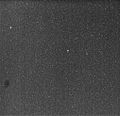
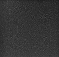
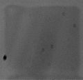
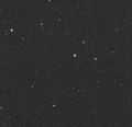
The pictures show the calibration using the example of an astronomical recording:
- The raw image shows numerous “ hot pixels ”, which lead to a very noisy image. Faint stars are lost in this noise. Dark spots in the raw image are caused by dust in the CCD camera.
- The dark image was taken with the same exposure time and operating temperature as the raw image, but with the camera shutter closed . It thus records the dark current that has accumulated during the corresponding exposure time .
- The white image was taken with the instrument aimed at a uniformly lit area. It detects irregularities in the illumination of the image (e.g. due to dust) and in the sensitivity of the individual pixels.
- These defects have been corrected in the calibrated image. Faint stars can also be seen here. The calibrated image can be used for quantitative analysis, for example for measuring the apparent brightness of the stars. Without calibration, such a measurement would lead to incorrect measured values.
Raw image
Dark image
White screen
Calibrated image


Irregularities in the CCD window
In the case of coherent light in particular, improper processing of the CCD window, which protects the sensor from dust, can lead to undesirable interference patterns. This problem can be solved by not building the window plane-parallel , but by tilting one side of the window at a certain angle with respect to the other side. If a beam falls on the front of the window, it emerges slightly inclined on the back towards the sensor, whereby the exact exit angle can be calculated with Snellius . However, the beam is also reflected alternately on the front and back within the window and exits the window again in the direction of the sensor at other points. If, for the sake of simplicity, only two partial rays emerging from the window are observed, the wave fronts of the rays form a moiré pattern. With a suitable choice of the angle of inclination, the maxima stripes of the pattern move so close together that they can no longer be resolved by the individual pixels.
Statistical errors and noise
The most important parameters for characterizing the quality of CCD chips are:
- The quantum yield , i.e. the probability that an incident photon will trigger an electron. The quantum yield of CCDs depends on the wavelength of the light and can be over 90% ( photographic film for comparison: 5% to 10%).
- The dark current of the light-sensitive cells. The dark current is strongly temperature-dependent and, due to its statistical properties, leads to dark current noise. It is different for each pixel and is a source of image noise . Individual “ hot pixels ”, ie pixels with a particularly high dark current, can also occur.
- The number of charges that can be stored in a pixel ( full well capacity or well depth ).
- The behavior when overexposure creates more charge in individual pixels than can be stored. If the charge transfers to neighboring pixels, it is called “ blooming ”. Many CCD cameras avoid this effect by diverting the excess charges ("anti-blooming gate"), but this can also cause charge to be lost before a pixel is really full. The relationship between the amount of light and the charge is then no longer linear, and precise measurements are no longer possible.
- The efficiency of the charge transfer to the readout amplifier ( Charge Transfer Efficiency ).
- The noise of the readout amplifier (readout noise ).
In the case of highly sensitive cameras, dark current and noise are reduced by cooling the CCD chip. The dark current noise can, for example, be reduced to below three electrons per pixel and hour by cooling with liquid nitrogen.
Size information
The size of the photosensitive area on the chip is very important for the image quality. With the same resolution (number of pixels), the area of the cells is proportional to the chip area. The larger the cells, the more photons hit per cell, which increases the sensitivity to light. Since not all interfering signals increase with the area of a cell, a larger chip has a better signal-to-noise ratio . In addition, larger cells can collect more electrons and thus have a larger dynamic range.
In addition to the direct metric specification of the active area (e.g. 16 mm × 24 mm), the tradition from the time of the image pick-up tubes has been preserved in which the outer diameter of the glass bulb in inches (e.g. 2/3 ″) is used to indicate the size has been used. However, the light-sensitive area of the tubes was significantly smaller than the outer diameter of the tubes: For example, a 1 ″ tube had an active area with an image diagonal of approx. 16 mm. By definition, a 1 ″ CCD chip has the same screen diagonal as a 1 ″ tube.
Common sizes for classic camera tubes as for CCD video sensors are for professional video cameras 2/3 "(11 mm diagonal) and 1/2" (8 mm diagonal), for prosumer devices 1/3 "(ca 5.5 mm diagonal) and even smaller sensors (1/4 ″ or 1/6 ″) for consumer devices or cell phone cameras. Small digital cameras often use 1 / 2.3 ″ sensors (approx. 7 mm diagonal), digital SLR cameras usually use a format similar to that of APS-C (approx. 28 mm diagonal) or, in the higher price range, a format similar to that of the 35mm format of photography on film.
Applications

Image acquisition
CCD sensors can be manufactured for visible wavelengths as well as for near infrared , UV and X-ray ranges . This extends the spectrum for special applications from 0.1 pm to around 1100 nm. The limit to long wavelengths is limited by the band gap of the semiconductor material (approx. 1.1 eV for Si and 0.66 eV for Ge). They can therefore be used in a variety of ways in natural sciences and technology. In astronomy in particular, they largely ousted other image receivers, such as photo plates , at an early stage, as their high sensitivity also allows very faint objects to be observed. Further advantages are their broad spectral sensitivity, their high dynamic range (i.e. the ability to capture very weak and very bright areas of an image at the same time) and the fact that the image information is obtained digitally, which for example in photometry (brightness measurement) and the application sophisticated image editing methods is beneficial.
CCD digital cameras have also caused a revolution in general photography . With an increase in the number of pixels, the possible uses of CCD image sensors expanded to include practically all photographic applications. Professional analog photo cameras have already been replaced in many areas by CCD sensors with 5 to 18 megapixels , which is all the more true for digital (single-lens reflex) cameras in medium format and increasingly in small format with 30 and more megapixels.
CMOS vs. CCD
In photo technology , CMOS sensors , with which only cheap “low-end” devices were previously equipped, replaced CCD sensors in the high-quality sector after 2005. Major CMOS disadvantages (noise, lower sensitivity) have largely been minimized or undercut to a comparable level, so that CMOS sensors have completely displaced the CCD sensors in the area of digital single-lens reflex cameras (e.g. Canon EOS-1Ds 2002, Nikon D2X 2004, Nikon D300 2007). With (for the area of application) comparable image quality, the advantages of CMOS sensor technology predominate (faster and area-controlled reading, hardly any blooming, etc.). CCD sensors, on the other hand, are found in digital backs and medium format cameras with very high resolutions (40 megapixels and larger), which can fully exploit their advantages here. Even in high-quality digital compact and bridge cameras , CCD sensors were used almost exclusively until 2010 ( Canon Powershot S100 with CMOS in 2011, Powershot G1X 2012).
Video technology
In video cameras , CCD sensors are replacing the older tube principle ( Ikonoskop , Vidicon ). The classical resolution of the video cameras to PAL - or NTSC - standard is 440,000 pixels (CCIR / PAL) or 380,000 pixels (EIA / NTSC) and frame rates of 25 Hz (CCIR / PAL) or 30 Hz (EIA / NTSC).
Intensified CCD, Gated CCD
CCDs can be operated with an image intensifier in front of them and are then referred to as intensified CCD (iCCD). To do this, the light first hits a photocathode; the electron stream released is multiplied in a microchannel plate (MCP) , for example , and hits a fluorescent screen. From there, the light is directed to the CCD via fiber optics, for example . Because of the high sensitivity of today's CCDs, intensified CCDs do not offer any gain in sensitivity with long exposure times (the quantum yield of the photocathodes is even lower than that of the best CCDs). Since the most sensitive CCDs have a relatively low readout speed, iCCDs can be advantageous at high frame rates (e.g. video). Intensified CCDs also enable very short exposure times of up to 0.2 ns , which are by no means achievable with a CCD alone. To do this, a short voltage pulse is applied to the microchannel plate. This arrangement is known as a gated CCD.
EBCCD
CCDs are not only sensitive to electromagnetic radiation, but also to ionizing particle radiation, since they also generate electron-hole pairs. “ Back-illuminated ” CCDs, which are used as sensors for incident electrons, are also known as ebCCD ( electron bombarded CCD ). One application of these sensors is as a residual light amplifier: The electrons come from a photocathode and are accelerated to an ebCCD sensor by means of an applied voltage, so that several electron-hole pairs are generated for each incident electron.
literature
- Gerald C. Holst: CCD arrays, cameras and displays. JCD Publishing, Winter Park 1996, ISBN 0-9640000-2-4 .
Web links
- (Digital Photography Review) ( Memento from February 5, 2013 in the Internet Archive )
- Detailed description of the semiconductor physics of MOS-CCDs (Ulm University)
- Modern CCD techniques (English), compiled by Andor
- True-to-scale overview of the sensor sizes of digital cameras ( Memento from November 21, 2013 in the Internet Archive )
- CCD simulator of Nebraska-Lincoln University (English)
- Nobel Prize in Physics for inventor of the CCD sensor
- Detailed site about the early use of CCD sensors in digital cameras and still cameras (English)
Individual evidence
- ^ WS Boyle, GE Smith: Charge coupled semiconductor deadapted devices . In: The Bell system technical journal (BSTJ) . Vol. 49, 1970, ISSN 0005-8580 , pp. 587-593 ( PDF ).
- ↑ GF Amelio, MF Tompsett, GE Smith: Experimental Verification of the Charge Coupled Device Concept . In: The Bell system technical journal (BSTJ) . tape 49 , 1970, ISSN 0005-8580 , pp. 593-600 .
- ^ The Nobel Prize in Physics 2009. Retrieved April 18, 2018 .
- ^ DF Barbe: Imaging devices using the charge-coupled concept . In: Proceedings of the IEEE . Vol. 63, no. 1 . New York 1975, p. 38-67 . ISSN 0018-9219
- ↑ The CCD Image Sensor, Thomson-CSF Division Silicon, application brochure DTE-145