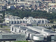
CEA-Leti
CEA-Leti ( Laboratoire d'electronique des technologies de l'information ) is a research institute for electronics and information technology based in Grenoble . It is one of the largest institutes for application-oriented research in microelectronics and nanotechnologies in France .
history
CEA-Leti was founded in Grenoble in 1967 as a subsidiary of Commissariat à l'énergie atomique et aux énergies alternatives (CEA). Since then, around 250 CEA-Leti patents have been registered annually. The institute administers around 1700 inventions that are protected by patents. The institute employs 1200 people, trains 220 students and accepts 200 members from research and industry partners. It has production lines for 200 mm and 300 mm wafers, 11,000 m² of clean room laboratories and equipment for the investigation of nanotechnology, chemistry, biology and photonics.
tasks
The institute's task is to create innovations and pass them on to industry, which aims to improve the quality of life worldwide through the development of technologies and products. Leti works by helping companies bridge the gap between fundamental research and end products. Leti also helps start up new companies by providing its partners with intellectual property and thus creating a performance advantage.
Important data
- 1967: Leti was originally created to meet the electronic needs of the French Atomic Energy Commission ( CEA ).
- 1972: Spin-off EFCIS becomes STMicroelectronics
- 80s: Leti opens several new buildings and cleanrooms and becomes known for his work in infrared technology and magnetometry. It also begins to develop micro- and electromechanical systems ( MEMS ), etc. a. Develop accelerometers and weight sensors. Leti patented the first silicon accelerometer.
- 1991: Leti agrees with CNET, the French Center for Telecommunications (Center National d'Etudes des Telecommunications), to create the Grenoble Submicron Silicon Initiative (GRESSI).
- 1992: The subsidiary company Soitec is founded to market silicon-on-insulator and other semiconductor and substrate technologies.
- 1997: The subsidiary Tronics Microsystems is founded to market customer-specific MEMS production technologies.
- 2002: Leti developed the first silicon MEMS gyrometer and transferred it to 200 mm discs.
- 2003: The silicon accelerometer process was referred.
- 2006: Leti, in collaboration with local and state governments and the Grenoble Institute of Technology (INPG), presents Minatec , the Grenoble-based research and development campus . This is intended to promote public and private partnerships geared towards micro- and nanotechnology.
- 2008: Alliance with Caltech (NanoVLSI Alliance).
- 2009: Alliance with IBM More Moore CMOS.
- 2011: First 3D 300 mm R&D line with all capabilities.
Main activities / applications
- Micro and nanotechnologies for microelectronics
- Micro and nanotechnologies for biology and health
- Development and integration of microsystems
- Imaging technology for medicine and security
- Wireless and Smart Devices
- Space and science
- Energy, transport and the environment
Partnerships
The researchers work in close relationships with industrial partners from around the world in targeted strategic partnerships to accelerate the development and commercialization of new technologies. Leti is also involved in several collaborative research initiatives such as:
- IBM 's semiconductor Joint Development Alliance
- The Alliance for Nanosystems VLSI (with the Californian Technology Institute - Caltech )
- The MicroMachine Center (with the Japanese Ministry of Economy, Trade and Industry)
- CEA-Leti and the Nokias Research Center
- IMAGINE, maskless lithography
