Flat (wafer)

A match head as a yardstick
A flat ( English for flat ) is a straight edge on the side of a wafer . It is used for wafer positioning in production systems for semiconductor technology .
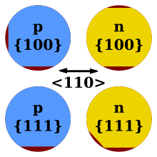
The flat is well on the crystal orientation of the single crystal oriented wafers. For a standard {100} wafer, the flat is attached in orientation {110}. The crystal orientation ( crystal structure analysis ) is determined with the help of X-ray diffraction . The flats themselves are ground into the ingot (elongated semiconductor single crystal , for example made from silicon rod ) using CNC- controlled grinding machines . Depending on the quality, the position of the flat is 0.5 ° or better to the desired crystal orientation; the position is given in degrees and seconds .
Another, somewhat smaller flat, the so-called secondary flat, is sometimes used for the extended identification of wafers. The doping and crystal orientation of the wafer can be identified by the position of this flat (see illustration).
Flats up to wafers with a diameter of 150 mm (“6 inches”) are used. For larger wafers (200 mm and 300 mm diameter), notches are used in combination with a barcode that contains further information. This method requires significantly less area on the wafer, which is now available for the production of the circuits.
Web links
- Your Guide to SEMI Specifications for Si Wafers. (PDF; 150 kB) Virginia Semiconductor, June 2002, accessed on September 20, 2010 (English, contains information on the size of the flats for different wafer sizes).

