Wafer
As wafer [ ˈweɪfə (r) ] ( English for "thin biscuit" or "thin slice of bread") are circular or square, about one millimeter thick slices in microelectronics , photovoltaics and microsystem technology . They are made from monocrystalline or polycrystalline ( semiconductor ) blanks, so-called ingots , and are usually used as a substrate (base plate) for electronic components , including for integrated circuits (IC, “chips”), micromechanical components or photoelectric coatings. In the production of microelectronic components, several wafers are usually combined into one lot and processed directly one after the other or also in parallel (see lot production ).

construction
In most cases, a disk is made of monocrystalline silicon , but other materials such as silicon carbide , gallium arsenide and indium phosphide are also used. Glass wafers with a thickness in the 1 mm range are also used in microsystem technology .
The discs are manufactured in different diameters. The main wafer diameters currently used differ depending on the semiconductor material and the intended use (silicon: 150 mm, 200 mm and 300 mm - 450 mm are under discussion; gallium arsenide : 2 inches , 3 inches, 100 mm, 125 mm and 150 mm - 200 mm technically feasible). The larger the wafer, the more ICs can be accommodated on it. Since the geometric scrap is smaller with larger wafers, the ICs can be produced more cost-effectively (see yield (semiconductor technology) ). In order to maximize the yield, the wafers are produced in clean rooms .
| designation | exact diameter (mm) | typical thickness (mm) | Launch (year) |
|---|---|---|---|
| 1 inch wafer | ? | ? | 1960 |
| 2 inch wafer | 50.8 | 0.275 | 1971 |
| 3 inch wafer | 76.2 | 0.375 | 1973 |
| 4 inch wafer | 100 | 0.525 | 1976 |
| 5 inch wafer | 125 | 0.625 | 1982 |
| 6 inch wafer | 150 | 0.675 | 1988 |
| 8 inch wafer | 200 | 0.725 | 1990 |
| 12 inch wafer | 300 | 0.775 | 1997 |
| 18 inch wafer | 450 | 0.925 (according to spec.) | still unknown |
The manufacturing costs of unstructured wafers depend on the diameter and the material (silicon, germanium , gallium arsenide, etc.) as well as the manufacturing process (see below). The costs for processed wafers - so-called structured wafers - increase significantly with the number of process steps. Even after the production of STI structures, the costs compared to unstructured wafers have at least doubled. In addition to the number of process steps carried out, the costs also depend significantly on the structure size used. Computer chips on an average 200 mm wafer with a structure size of 90 nm ( 90 nm technology ) cost around 850 euros per wafer in mid-2008. The production costs of top products (on 300 mm wafers), AMD graphics cards in 28 nm technology , and Intel processors in 22 nm technology , however, are significantly higher. Depending on the chip size, a few dozen to a few hundred chips can be produced on such a wafer. These costs do not include expenses that arise after the chip has been manufactured, for example packaging the chips in housings.
Manufacturing
Wafer production begins with a block of semiconductor material called an ingot . Ingots can have a monocrystalline or polycrystalline structure and are usually produced using one of the following processes:
- Zone melting process
- Czochralski method , u. a. the Liquid Encapsulated Czochralski process (LEC process)
- Bridgman-Stockbarger method
- Vertical Gradient Freeze (VGF)
- Pedestal procedure
- Block casting process or Bridgman process with a controlled melting and cooling process for polycrystalline silicon
All of these processes ultimately produce more or less cylindrical or square single or polycrystals that have to be sawed into slices, the wafers, across their longitudinal axis. Inner hole cutting was developed to optimize the precision for this special cut with as little waste as possible . The cutting blades carry the cutting teeth (possibly cutting diamonds ) on the inside of an inner bore, which must be slightly larger than the diameter of the blank. In the meantime, wire sawing , which was originally only developed for solar wafers, has become more and more established.
Special wafer designations can be found in the literature, which, among other things, indicate which manufacturing process was used. For example, wafers that were manufactured using the Czochralski process are referred to as CZ wafers. Analogous to this, the term FZ wafer is used for wafers that were manufactured using the float zone process.
For most applications, the surfaces of the wafers must be polished to an optically reflective finish. For this purpose, the wafers are first lapped and then treated with a chemical-mechanical polish until the required surface roughness (a few nanometers ) is achieved. Other important geometry parameters of wafers are the global thickness fluctuations ( total thickness variation , TTV), the type and size of the warp or warp ( wafer bow ) and much more.
Labelling
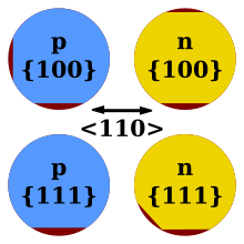
Since the exact position in the processing machine is important for the processing of the wafers, the wafers (for gallium arsenide up to 125 mm in diameter, for silicon up to 150 mm in diameter) are marked with so-called “ flats ”. With the help of a primary and possibly a secondary flat, it is shown which angular orientation is present and which crystal orientation the surface has (see figure). For larger wafers (for silicon with a diameter of 150 mm or more), so-called notches are used instead of flats . They offer the advantage of more precise positioning and, above all, cause less waste.
Nowadays, a unique wafer identification is also written as a barcode , OCR- readable text and / or data matrix code by laser at a point near the notch on the edge of the underside of the wafer.
In photovoltaics
In photovoltaics, two types of wafers are generally distinguished: polycrystalline (also called multicrystalline) and monocrystalline wafers. Both types are manufactured by sawing the appropriate ingots . Polycrystalline ingots are made from cuboid polycrystalline silicon blocks, from which the shape of the wafer results (mostly square). Monocrystalline wafers, on the other hand, are cut from cylindrical monocrystalline ingots, as they are also used for microelectronic applications. They usually have a "pseudo-square" shape, i. H. with rounded corners. In contrast to square-cut wafers, there is less waste when producing the round monocrystalline ingots. Inefficient, wasteful processes increase costs and worsen the environmental balance. In addition, the scrap is contaminated (and forms a suspension ) by the cutting aids and the wire abrasion and can only be recovered with difficulty. Other processes such as “ Edge-defined Film-fed Growth ” (EFG) from Schott Solar or “ String Ribbon ” (SR) from Evergreen Solar make it possible to pull very thin wafers directly from the melt. The wastewater, energy and waste-intensive wire sawing is no longer necessary. The wafer thickness is usually much thinner than in microelectronics, approx. 200 µm in current mass production. No polishing processes are used. In several subsequent processing steps, solar cells and, in turn, solar modules are produced from the wafers .
Web links
Individual evidence
- ↑ wafer noun. In: Oxford Advanced American Dictionary at OxfordLearnersDictionaries.com. Retrieved October 25, 2019 .
- ↑ wafer. In: Merriam-Webster. Retrieved October 25, 2019 .
- ↑ Your Guide to SEMI Specifications for Si Wafers. (PDF; 150 kB) Virginia Semiconductor, June 2002, accessed on September 20, 2010 (English).
- ↑ Mark LaPedus: Industry Agrees on first 450-mm wafer standard . EETimes.com, October 22, 2008.
- ^ Graham Pitcher: In the space of five years, it looks like 450mm manufacturing has become surplus to current requirements. In: newelectronics.co.uk. June 28, 2016, accessed December 14, 2016 .
- ↑ Marc Sauter: Contract manufacturer: Intel develops three 10 nm processes and opens up to ARM. In: golem.de. August 17, 2016, accessed December 14, 2016 .
- ↑ TSMC 2008 Second Quarter Investor Conference, July 31, 2008 ( PDF )
- ↑ Entry multicrystalline ingot = multisilicon in the glossary ( memento of August 11, 2011 in the Internet Archive ) on silicon wafer production by Swiss Wafers, accessed on April 16, 2010.
- ↑ Sami Franssila: Introduction to Microfabrication . John Wiley and Sons, 2010, ISBN 978-0-470-74983-8 , pp. 274–275 (section: Wafer Mechanical Specifications ).
- ↑ Thickness, Shape and Flatness Measurement of Semiconductor Wafers (PDF; 44 kB). MTI Instruments Inc. (Overview of the wafer geometry characteristics).
- ↑ a b Joachim Frühauf: Materials in microtechnology . Hanser Verlag, 2005, ISBN 978-3-446-22557-2 , pp. 60 ( limited preview in Google Book search).
- ↑ Jörn Iken: Pulling or sawing - a system comparison solarenergie.com. December 4, 2006, accessed August 16, 2010.
- ^ Nicole Vormann: Sustainability and Social Responsibility in the Photovoltaic Industry. (Study) Murphy & Spitz, January 2010, accessed March 4, 2010 .


