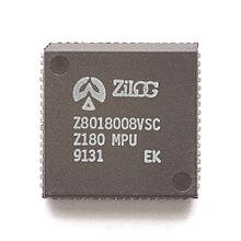
Zilog Z180
The Zilog Z180 is an 8-bit microprocessor that was developed in 1985 by Hitachi under the designation HD64180 . Later the company Zilog Inc. built the chip almost unchanged under the name Z180.
Command structure
The Z180 has a processor core that is completely code compatible with the Z80 . For the first time came here microcode technology with execution pipelining used. A number of commands require fewer machine cycles than the original Z80. A special interrupt , Reserved Instruction Trap , is triggered when an invalid command is detected. The undocumented commands popular with some Z80 programmers are therefore taboo for the Z180. Special instructions for addressing the internal registers and a multiplication command have been added.
Periphery
The success of the Z180 is mainly due to the fact that a number of peripheral components are already integrated on the chip. These are in detail:
- Clock generator. Only one crystal and two capacitors are required.
- Memory management ( Memory Management Unit MMU) for 1 MB of RAM.
- Two DMA controllers with memory <-> memory and memory <-> IO transfers. The DMA controllers support the full 1 Mbyte address space.
- Programmable wait state generator, separate for memory and IO access
- Programmable DRAM - Refresh controller
- Two asynchronous, serial full duplex interfaces ( UART ) with programmable baud rate generator for transmission rates from 300 to 38400 baud and support for modem control lines
- A clocked, serial high-speed interface for setting up multiprocessor systems
- Two 16-bit programmable timers
- Two external universal interrupt inputs
Memory management
Since the Z80 can logically address a maximum of 64 kbytes, the MMU manages the main memory via so-called memory banks. There are three areas:
- Common Area 0
- Bank Area
- Common Area 1
The MMU shows the physical memory in 4 kByte blocks in the logical address space. Common areas 0 and 1 are each at the lower and upper end of the logical address space and are normally assigned to fixed physical memory areas. If necessary, the program can switch the allocation of the logical memory in the bank area in between.


