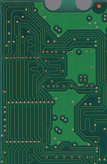
Solder mask
Solder mask , solder mask , Soldermask or soldermask met on a printed circuit board for electronic circuits different functions. It serves to protect the copper conductor tracks from corrosion , protection from mechanical damage and prevents wetting of the areas on the circuit board covered with it during soldering . In addition, solder mask improves electrical properties such as dielectric strength . It was developed especially for wave soldering systems in order to avoid solder bridges and to reduce the consumption of solder . The most common color is green, but other colors such as red, blue or white are also possible. Epoxy resin , for example, can be used as a material for solder mask .
The solder mask should harmonize with the flux and cleaning agents used.
Application process
The application methods are determined by the type of solder mask. There are two broad groups of solder resists.
- Photoimageable solder resists ( LPI , liquid photoimageable soldermask )
- Solder masks that cannot be photo-structured
The non-photostructurable solder resists are cured either thermally or by means of UV light . They are applied by screen printing using structured screens .
The photo-structurable solder resists are viscous liquids or photopolymer foils in the form of a dry film. All photo-structurable solder resists are negative working. After application, they must be dried, exposed and developed.
The photopolymer films are applied by lamination . Its importance has declined very much at the moment.
In practice, the following methods are used to coat circuit boards with solder resists:
- Screen printing ( screen printing )
- Spraying ( spraying or jet dispensing )
- Contactless dosing ( jetting )
- Curtain coating ( curtain coating )
- Roll coating ( roller coating )
There are different variants of each of these processes with advantages and disadvantages, so that one cannot speak of an optimal coating process.
Screen printing process
In the screen printing process, the solder mask is pressed through a screen using a squeegee . A distinction can be made between vertical and horizontal screen printing systems.
Screen printing is carried out horizontally on one side or vertically on both sides. Horizontal double-sided coating can also be carried out on a needle bed using screen printing.
Spray process
Spray processes are also divided into vertical and horizontal processes according to the orientation of the circuit board. A distinction is also made between electrostatic and conventional spraying.
Inkjet technology
Inkjet technology is a new method of applying solder resists. This process is still under development.
The two circuit board manufacturers Würth Elektronik and FELA GmbH have been promoting research since the beginning of 2017 and in October 2017 delivered the first series orders under the name "s.mask" - a process that is independent of print and lacquer manufacturers. In connection with the new technology, we no longer speak of a mask or a coating, but of modeled surfaces. With appropriate data preparation it is z. B. already possible to realize different values for the dielectric strength on a circuit board or to form a kind of solder mask already on the circuit board with "soldermask defined pads".
literature
- Reinard J. Klein Wassink: Soft soldering in electronics . 2nd Edition. Eugen G. Leuze, Saulgau 1991, ISBN 3-87480-066-0 .
- Wolfgang Scheel (Hrsg.): Assembly technology of electronics . Verlag Technik et al., Berlin et al. 1997, ISBN 3-341-01100-5 .

