Quantum well
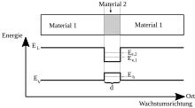
Under a quantum well ( English quantum well ) is defined as a potential profile that limits the freedom of movement of a particle in one dimension (typically in the z-direction), so that only a planar region (x, y-plane) can be filled. The width of the quantum well largely determines the quantum mechanical states that the particle can assume. This leads in particular to the formation of energy levels (sub-bands), i. This means that the particle can only take on discrete (potential) energy values.
Manufacturing
In semiconductor technology , quantum wells are produced by embedding a layer of a semiconductor with a smaller band gap (e.g. GaAs ) between two layers of a semiconductor with a larger band gap (e.g. AlGaAs ). For this reason, the resulting structure is often referred to as a quantum film . A widely used method for producing such structures is molecular beam epitaxy , which enables layer thickness control down to the range of individual layers ( monolayer ). In order to achieve good layer quality, it must be ensured , among other things, that the materials used are lattice-compatible , i. that is, have a sufficiently similar crystal structure (including lattice constant ).
Applications
Due to the two-dimensional nature of the quantum well, the electrons and holes in it have a different density of states than in the three-dimensional crystal. Targeted doping allows (highly mobile) two-dimensional electron systems to be grown. B. in HEMTs (English high-electron-mobility transistor ). Further applications are e.g. B. the quantum cascade laser , diode laser or quantum well infrared photodetector .


