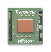
Transmeta Efficeon
The Efficeon , developed under the code name Astro , is a particularly energy-saving processor family from Transmeta , which should be used above all for embedded systems , notebooks and low-noise workstation computers that do not require active cooling.
Like its predecessor, Crusoe , the 256-bit processor relies on code morphing technology and the VLIW architecture. However, the efficiency of code morphing has been significantly improved. So far, this technology has emulated the x86 processor architecture including Intel's SSE2 instruction set extension. In theory, however, other architectures could also be emulated.
Model data
TM8300
- L1 cache: 64 + 128 KB (data + instructions)
- L2 cache: 512 KB with processor clock
- MMX , SSE , SSE2 , LongRun ! 2
- VLIW with code morphing technology
- Northbridge integrated in the CPU
- Packaging:
- 783 pin BGA
- Release DATE: June 2004
- Manufacturing technology: 130 nm at TSMC
- The size: 119 mm² with an unknown number of transistors
- Clock rates: 1000 and 1100 MHz
TM8500
- L1 cache: 64 + 128 KB (data + instructions)
- L2 cache: 512 KB with processor clock
- MMX , SSE , SSE2 , LongRun ! 2, NX-Bit
- VLIW with code morphing technology
- Northbridge integrated in the CPU
- Packaging:
- 783 pin BGA
- Publication date:
- Manufacturing technology: 90 nm at Fujitsu
- The size: 68 mm² with an unknown number of transistors
- Clock rates: 1000–1700 MHz
TM8600 / TM8620
- L1 cache: 64 + 128 KB (data + instructions)
- L2 cache: 1,024 KB with processor clock
- MMX , SSE , SSE2 , LongRun ! 2
- VLIW with code morphing technology
- Northbridge integrated in the CPU
- Packaging:
- 783 pin BGA (TM8600)
- 592 pin BGA (TM8620)
- Release DATE: June 2004
- Manufacturing technology: 130 nm at TSMC
- The size: 119 mm² with an unknown number of transistors
- Clock rates: 1000–1200 MHz
TM8800 / TM8820
- L1 cache: 64 + 128 KB (data + instructions)
- L2 cache: 1,024 KB with processor clock
- MMX , SSE , SSE2 , SSE3 , LongRun ! 2, NX-Bit
- VLIW with code morphing technology
- Northbridge integrated in the CPU
- Packaging:
- 783 pin BGA (TM8800)
- 592 pin BGA (TM8820)
- Release DATE: September 2004
- Manufacturing technology: 90 nm at Fujitsu
- The size: 68 mm² with an unknown number of transistors
- Clock rates: 1000–1700 MHz


