
Zener diode

A Zener diode (formerly also Zener diode) is a diode that is designed to be operated permanently in reverse direction in the range of the breakdown voltage . The level of this breakdown voltage U BR is the main characteristic of a Zener diode and is specified in the data sheet. This is achieved by a heavily doped p + and a heavily doped n - layer. The strong recombination of both layers leads to a very small barrier layer thickness and thus to high field strengths in the area of the barrier layer.
In the past, these diodes were named after the American physicist Clarence Melvin Zener , who discovered the Zener effect (electrons tunnel through the barrier layer). The name Zener diode has been recommended since the 1970s because the Zener effect is only responsible for low breakdown voltages. In the forward direction they behave like normal diodes. In the reverse direction, Z diodes are blocking at low voltages, just like normal diodes. From a certain reverse voltage , the so-called breakdown voltage, the current increases by many orders of magnitude within a few hundred millivolts. This process does not depend on the history (e.g. in contrast to the diac ), i.e. In other words, when the voltage is reduced, this current also decreases again. Zener diodes are therefore suitable for voltage stabilization (small voltage change with large current changes, clear I (U) characteristic) and for voltage limitation.
Due to the small thickness of the barrier layer, Zener diodes have a large barrier layer capacitance and they have a lot in common with capacitance diodes .

Breakthrough effects

The breakdown voltage or Z-voltage (mostly U BR from br eakdown voltage , more rarely also U Z ) is in the range 2.4–200 V (extended range: 1.8–300 V) for Z diodes . Any higher voltages can be achieved through series connection, bidirectional Zener diodes are obtained through anti-series connection.
If U Z is now applied to the diode in reverse direction, the current through the diode results from the formula:

At low Z-voltages (below 3 V), the Zener effect with its characteristic negative temperature coefficient (approx. −0.09% / K) and its comparatively flat breakdown is dominant for the breakdown. With higher Z-voltages (above 5 V) of the dominated avalanche breakdown effect (engl. Avalanche effect ) with its positive temperature coefficient (about +0.11% / K) and the much steeper breakthrough. At breakdown voltages between 4.5 V and 5 V, the temperature coefficients largely compensate each other. Due to the different steepness of the characteristics of the two effects, the compensation is current-dependent and works largely perfectly for a certain operating current. For higher currents, this point shifts to lower voltages.
Clarence Zener was already aware of this problem, so he suggested dividing the diodes, initially generally known as Zener diodes, into Zener diodes (with breakdown voltages below 5 V) and Zener diodes (with more than 5 V). In everyday use, the term Z-diode has established itself as a generic term for Zener and avalanche diodes .
With the Zener effect, the electrons tunnel through the extremely thin barrier layer, although there are actually no charge carriers. In the event of an avalanche breakdown, the few electrons present are accelerated by the electric field and release additional electrons from the crystal lattice through collisions. As a result, there is an avalanche-like increase in charge carrier concentration and thus an avalanche-like increase in conductivity.
Temperature dependence

The specification of the Z voltage U Z generally refers to 300 K. The temperature coefficient or TC indicates the relative change in the Z voltage as a function of the temperature T :

- at I D = const.

In data sheets, the temperature coefficient is often stated in relation to the voltage in millivolts per Kelvin. The conversion is done as follows:

Below 7 V, the temperature coefficient depends significantly on the diode current, which is why the nominal current must always be specified.
Common values are:
| TC (U Z ) | U Z |
|---|---|


The Z-voltage and its change as a function of the temperature is calculated using the following formulas:

![U_ {Z} (T) = U_ {Z} + \ Delta U_ {Z} (T) = U_ {Z} \ cdot \ left [1 + k _ {\ vartheta} \ cdot \ left (T-300 \, { \ mathrm {K}} \ right) \ right]](https://wikimedia.org/api/rest_v1/media/math/render/svg/2e908e7129ac493e15265b30521e126d1cd30d8b)
The Zener effect has a negative temperature coefficient, the avalanche effect a positive one. At approx. 5 V, both coefficients are about the same and cancel each other out. For particularly long-term stable references, a series connection of a Zener diode with 6.2 to 6.3 V and a temperature coefficient of +2 mV / K and a normal silicon diode (or base-emitter path of a transistor) in the forward direction with −2 mV / K was used on the same chip, which cancel out the temperature coefficients. Bandgap references are not used as reference voltage sources in integrated circuits, however , because these are much cheaper to integrate on the chip (Zener diodes would require many additional process steps), are much more precise and have more long-term stability, and above all at low voltages (e.g. at 3 V).
Current-voltage characteristics are occasionally given in data sheets , i.e. H. the characteristic curves of the diodes at 25 ° C and 125 ° C.
Equivalent circuit diagram

In the equivalent circuit is the differential resistance of the Zener diode; its value is typically in the range of a few ohms . The voltage source represents the Zener voltage of the diode.


Working point

The working point of the diode is the value pair of voltage and current that is assumed due to the external wiring. The working point of a Zener diode is at the intersection of the diode characteristic and the load resistance characteristic.
The diagram on the right shows the characteristic with a load-dependent supply voltage. Depending on the load, operating points are set with different voltages - the lowest voltage at full load and the highest voltage at the Zener diode when idling. Whereby the operating point thereby moves between the points 1 and 2 (control range), a corresponding variation of the Zener current I Z is caused.
The lower limit of the control range is determined by the kink in the characteristic and is approx. 10% of I max . The entire control range between points 1 and 3 can be used with a variable load resistance.
application
As a rule, Zener diodes are operated in reverse direction. They are used for voltage limitation, overload protection and, the most common area of application, for voltage stabilization. Common is z. B. the parallel regulation of a voltage for other electronic circuit parts that require a stable supply or input voltage. Another example is the Zener barrier . Furthermore, Z-diodes can be used very well as a generator for white noise , which is caused by the avalanche effect.

Voltage limitation with Zener diode
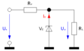
Voltage stabilization with Zener diode
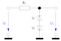
Symmetrical voltage limitation with antiserial zener diodes


In the circuit for voltage limitation, the Zener diode blocks voltages of . In this area, the output voltage results only from the series resistance and - in the case of voltage stabilization - the load resistance .


If the Zener diode conducts at, the maximum Z voltage is applied to the load resistor .


This results in the following formula:

Using the example of a Zener diode with a Zener voltage of U Z = 10 V, it would look something like this:

This results in a smoothing (limitation) of the actual input voltage and thus a stabilization of the output voltage. These are described using the smoothing factor G and the stabilization factor S , which result from the following formulas:

r z is the differential resistance of the Zener diode, which should be as small as possible. With the typical values r z = 5 Ω and R v = 1000 Ω, fluctuations in the input voltage (including the residual ripple ) are reduced to 0.5%.
Relative stabilization factor S :

The symmetrical voltage limitation works similarly to the voltage limitation described here with only one Zener diode. However, they also limited negative input voltages - U Z . In addition, however, there is a voltage drop U D at the second Zener diode, which in this case is conductive. This behaves in the same way as the voltage drop of a conventional diode .
Voltage regulators , which can regulate the voltage much more precisely, provide a better option for voltage stabilization .
Labelling
.jpg)
The housing of Zener diodes usually has a ring on the cathode side. The marking thus corresponds to the conventions of other diodes.
See also
literature
- Ulrich Tietze, Christoph Schenk, Eberhard Gamm: Semiconductor circuit technology . 12th edition Springer, 2002, ISBN 3-540-42849-6 .
- Stefan Goßner: Basics of electronics . 11th edition, Shaker, 2019, ISBN 978-3-8440-6784-2 , Chapter 5: Stabilization circuit with Zener diode .
Web links
- Z-Diode extension course and the bandgap reference elektronik-kompendium.de
- The power zener diode made of zener diode and transistor elektronik-kompendium.de
Individual evidence
- ↑ Fluke Corporation (Ed.): Calibration: Philosophy in Practice . Everett, Washington 1994, ISBN 0-9638650-0-5 .