
diode


A diode is an electronic component that allows current to pass in one direction and blocks the flow of current in the other direction. This is why we speak of the forward direction and the reverse direction. The behavior was discovered in 1874 by Ferdinand Braun at point contacts on lead sulfide ( galena ).
The term diode is usually used for semiconductor diodes that work with a pn junction or a rectifying metal-semiconductor junction ( Schottky contact ). In semiconductor technology , the term diode only refers to silicon diodes with a pn junction, while other variants are identified by suffixes, for example Schottky diodes or germanium diodes . Designations such as valve cells , which were used for diodes in the then newly developed semiconductor technology and which go back to the analog function of a mechanical valve , are outdated .
Diodes are used, among other things, for rectification , the conversion of AC voltage to DC voltage . In addition, the semiconductor junction shows other useful properties that z. B. can be used in Zener , photo , light emitting diodes and semiconductor detectors .
Structure and physics of a semiconductor diode

The basis of the semiconductor diode is either a pn-doped semiconductor crystal (mostly made of silicon , but also germanium, see germanium diode or gallium arsenide ) or a metal-semiconductor junction (see Schottky diode ).
The conductivity of such a transition depends on the polarity of the operating voltage at the anode (p- doped ) and cathode (n- doped ), i.e. on the direction of current flow. The pn-junction (gray area) is a zone that is free of moving charge carriers , since positive charge carriers (so-called defect electrons or holes ) of the p-doped crystal and negative charge carriers (free electrons) of the n-doped crystal on the other Diffuse side of the pn junction and disappear there by recombination (see article pn junction ). The original sources of the charge carriers, the doping atoms, are stationary and now form a space charge as ions, the electrostatic field of which keeps the two types of charge away from each other and thus prevents further recombination. The diffusion voltage arises over the entire space charge zone . This can be compensated for by an externally applied voltage - depending on the polarity - then the pn junction becomes conductive, or it is reinforced, then it remains blocked.

pn junction

pn diode

Schottky diode


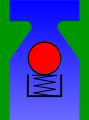
Mechanical replacement model of the diode
The easiest way to imagine the function of a rectifier diode in a circuit is like a check valve in the water circuit : If a pressure (a voltage) acts on this valve (diode) in the reverse direction, the flow of water (current) is blocked. In the forward direction, the pressure (voltage) must be high enough to overcome the spring force of the valve (= threshold or sluice voltage of the diode). This opens the valve (the diode) and the current can flow. This pressure, which is necessary in the mechanical model to overcome the spring force, corresponds to the so-called threshold voltage ( ) or minimum forward voltage drop in the case of a diode, which must be applied to the diode in the flow direction so that it is in the conductive state transforms. With ordinary silicon diodes this is around 0.6-0.7 V.


Closed ball check valve
Open ball check valve

Bicycle valve ; the internal pressure acts as a restoring force


The check valve behaves in turn according to the Shockley formula , which was developed to describe the semiconductor diode (see below under Ideal Diode ). The formula is therefore suitable for the approximate calculation of valves.
Electrical behavior
The analysis of electrical circuits requires a mathematical description of the diode. The graphical current-voltage characteristic , exact equations and simplified models are available for this.
Formula symbol
The detailed examination of a diode requires specific symbols. The following table simplifies the overview.
| character | description |
|---|---|
| Voltage on the diode | |
| Lock voltage (also called threshold voltage), diode conducts in the forward direction | |
| Forward voltage; Voltage across the diode in the forward direction ;
Corresponds to (same sign); Usage partly identical to |
|
|
Reverse voltage ; Voltage across the diode in the reverse direction (engl. Reverse voltage );
Corresponds to (rotated sign) |
|
| Breakdown voltage (engl. Breakdown voltage ) | |
| Current through the diode | |
| Reverse saturation current | |
| ; | Diffusion current ; Current through the diode in the forward direction (engl. Forward current ) |
| ; | Leakage current ; Current (engl. Through the diode in the reverse direction reverse current ) |
| Leakage saturation reverse current | |
| Breakdown current ; Current through the diode in the (reverse) breakdown (engl. Breakdown current ) | |
| Emission coefficient | |
| Temperature stress | |
| Bandgap voltage (Engl. Gap voltage ) | |
| Track resistance ; ohmic resistance of the semiconductor material | |
| Differential resistance | |
| or | Working point |
| Diode capacity | |
| Junction capacitance | |
| Diffusion capacity |


In addition, the following natural constants are important:
| character | description |
|---|---|
| Boltzmann constant | |
| Elemental charge |


Static behavior
The static behavior describes a diode with direct voltage and also applies approximately to alternating voltages with a low frequency, around 50 Hz mains voltage, but depending on the version also up to the MHz range. Redistribution processes in the pn junction caused by a changed voltage are not taken into account.
curve

The current-voltage characteristic curve best describes the static behavior of a diode. The characteristic curve is divided into three sections: the pass band, the stop band and the breakdown area.
As the characteristic curve shows, no noticeable current flows through the diode in the pass band despite the small voltage applied (based on the currents common in technology). The current in Si diodes only starts to increase noticeably from a voltage of around 0.4 V. From around 0.6 V to 0.7 V, the current increases sharply, which is why it is referred to as the lock voltage . With Schottky and germanium diodes, a significant current already flows at around 0.2 V and the lock voltage is around 0.3 V to 0.4 V.


A very low current flows in the blocking range, the so-called leakage current . Ge and Schottky diodes have significantly higher values than Si diodes.

Depending on the doping, the breakdown range of Si diodes begins at or from around −50 V to −1000 V and the diode becomes conductive in the reverse direction. The same applies to a Schottky diode at around −10 V to −200 V. This breakdown voltage is given with a positive sign. Through special doping , breakdown voltages of less than 5 V are achieved with Si diodes, which is particularly used with Z diodes .


Ideal diode / Shockley equation
Because of the non-linearity, simplifications are used that only approximate the behavior, but allow easier handling. In the simple model of the diode, this is viewed as an ideal check valve or as a switch, the position of which depends on the polarity of the applied voltage. The ideal diode is conductive in one direction without a voltage drop, in the opposite direction it is blocking without leakage current. The characteristic therefore consists of two half-lines on the coordinate axes. The ideal diode is described in the form of an equation


in the passband at in the restricted area at


The states and do not exist in this model.


If the lock voltage and the non-abrupt characteristic curve are to be included in the description of the behavior, as indicated below , with continued linear approximation, the equivalent circuit is expanded as shown in the adjacent figure. The directions of current and voltage are chosen as in the consumer counting arrow system . With the same sign of the two quantities, this voltage source behaves as a special feature like a consumer. This can be seen in the heating of the real diode.
An electronic circuit that, for example, takes on the function of a rectifier like an ideal diode for measuring purposes - without the shortcomings of the high lock voltage and the non-linear characteristic curve - is described under precision rectifier .
The characteristic curve of the diode in the pass band according to the Shockley equation (named after William Bradford Shockley ) comes closest to reality ; it is a special case of the Arrhenius equation .
-
- Saturation reverse current (short: reverse current)
- Emission coefficient
- Temperature stress at room temperature
- absolute temperature
- Boltzmann constant
- Elemental charge


There is a relative error of <1% if the second term in brackets is omitted. Then applies


and the Shockley characteristic becomes a straight line in a simple logarithmic representation .
On closer inspection, the diode current is composed of the diffusion current , taking into account the high current effect , the leakage current and the breakdown current :

Temperature dependence
The diode characteristic varies with temperature. There are two temperature-dependent terms in the Shockley equation:

![{\ displaystyle {I _ {\ text {S}} (T)} = {I _ {\ text {S}} (T_ {0})} \ cdot {\ exp \ left [\ left ({T \ over T_ { 0}} - 1 \ right) \ cdot {{U _ {\ text {G}}} \ over {nU _ {\ text {T}}}} \ right]} \ cdot {\ left ({T \ over T_ { 0}} \ right) ^ {\ frac {x} {n}} {\ text {with}} x \ approx 3}}](https://wikimedia.org/api/rest_v1/media/math/render/svg/b7bedec24646b2ad92a990ab05adcac924d148bc)
Are there
- the reverse current assumed to be known at the temperature ,
- the bandgap voltage ( gap voltage ).


The following applies to silicon . This voltage is used (often temperature-compensated) in the bandgap reference circuit to generate reference voltages .

In addition, the temperature dependence of the voltage must also be taken into account:

This temperature coefficient is constant enough in the relevant temperature range around 300 K to be able to take temperature measurements based on the approximately linear temperature dependence of the forward voltage.
In practice, the voltage of around 0.7 V can actually be used for many rough calculations as the value of the forward voltage of silicon diodes and pn junctions.
Diffusion current
The diffusion current occurs in the middle transmission range, where it dominates over the other effects. The formula results from the Shockley equation with:

With Schottky diodes, the emission current can be described with the same formula .
High current effect
The high current effect causes an increase from in the range of the mean currents to at for towards infinity. The knee current describes the limit to the high current range . As a result, less current flows and the characteristic curve has a flatter but still exponential course.


Leakage current (recombination current)
When a reverse voltage is applied , the electrons and holes are carried away to the respective contacts, thus enlarging the space charge zone and the diode should not conduct any current. In practice, however, a low current is still measured, the so-called leakage current (reverse current). It results from the diffusion of charge carriers through the space charge zone into the oppositely doped area, where they are then dissipated due to the applied voltage. The p-zone supplies electrons and the n-zone holes, which, as minority charge carriers, lead to the reverse current.

The following applies to the mathematical calculation:
![{I _ {{\ text {D, R}}}} = {I _ {{\ text {S, R}}} \ cdot \ left ({\ mathrm e} ^ {{{{{U _ {{\ text {D }}}} \ over {n_ {R} \ cdot U _ {{\ text {T}}}}}}} - 1 \ right) \ cdot \ left [{\ left (1 - {{U _ {{\ text {D}}}} \ over {U _ {{\ text {diff}}}}} \ right)} ^ {2} +5 \ cdot {10 ^ {{- 3}}} \ right] ^ {{m_ {{\ text {S}}} \ over 2}}}](https://wikimedia.org/api/rest_v1/media/math/render/svg/8b8a65191c4553b288251fb1f07b3d6c4c7f43c3)
With
- - leakage saturation reverse current
- - Emission coefficient in reverse direction
- - diffusion stress
- - capacity coefficient


The reverse current is strongly dependent on voltage and temperature and depends on the manufacturing technology as well as the purity and lack of impurities.
breakthrough

The reverse current of a pn diode with reverse polarity is generally low. However, if the voltage is increased further in the reverse direction , the reverse current increases slowly and then suddenly from a certain reverse voltage. This increase in reverse current is commonly referred to as “breakdown”, and the associated voltage is known as the breakdown voltage . The breakdown voltage of a diode generally depends on the semiconductor material and the doping and can be in the range between 50 and 1000 V for rectifier diodes.


with , the breakthrough knee current, and , the breakthrough emission coefficient.


This state is undesirable for most semiconductor diodes, since it destroys the component in conventional diodes due to the high power dissipation and the thin, constricted current flow channel. The cause of the breakthrough are very high electric field strengths . Three different mechanisms can be distinguished: the avalanche, the Zener and the thermal breakthrough.
The avalanche breakthrough (also called avalanche breakthrough or avalanche effect) is characterized by a multiplication of charge carriers through impact ionization. It is used, for example, with the IMPATT and suppressor diodes , the avalanche photodiode , as well as with Z diodes (also called Zener diodes ) of higher voltage ( see also under Avalanche diodes ). The avalanche breakdown is also permissible and specified for some types of rectifier diodes (avalanche rectifier diode, avalanche type), so that they are not destroyed in the event of one-off or periodic overvoltage events up to certain energies.
With line diodes, z. B. 1N4007, exceeding the maximum permissible reverse voltage - even briefly for a few microseconds - is not permitted. The avalanche current then flowing leads directly to the destruction of the barrier layer. For the operation of diode rectifiers on the network, surge arresters, e.g. B. varistors are required, which limit the mains overvoltage to a level permissible for the rectifier diodes.
In the case of the Zener breakdown , on the other hand, the energy bands are strongly shifted by special doping. When the breakdown voltage is exceeded - in this case one usually speaks of the Zener voltage - a tunnel effect occurs, which enables valence band electrons to switch from the valence band to the conduction band without absorbing energy. The Zener breakdown is used in Zener diodes up to about 5 volts and is used, among other things, to provide reference voltages.

The thermal breakdown describes the breakdown of the reverse voltage due to high temperature and the associated generation of charge carriers. As a rule, it leads to the destruction of the diode by diffusion processes.
Differential resistance
The differential resistance results from the tangent through the working point of the diode. It is also known as dynamic resistance. By using a straight line instead of the actual exponential function, the required calculation steps are considerably simplified.


Working point: A
With large currents it becomes very small and the sheet resistance becomes increasingly apparent. This is a real resistance and is mainly due to the conductivity of the base material of the diode chip. It is in series in the equivalent circuit .
The equivalent circuit with and is only suitable up to frequencies of 10 to 100 kHz, depending on the type of diode. At higher frequencies, such as those that occur when switching on and off, the capacitive properties and the reverse recovery time of the diode must also be taken into account.
Track resistance
The sheet resistance is caused by the electrical resistance of the semiconductor material and the resistance of the connection on the semiconductor. The rail resistance is taken into account by the following formula:


Static small signal model

The static small signal model is used to dimension the operating point setting of simple circuits. This corresponds to the differential resistance already mentioned (see above). In addition, there is possibly also the rail resistance.

For operation around the reverse breakdown, i.e. as a Z-diode, the parameter is used to model the behavior.


Dynamic small signal model
For AC applications, one must also take into account the capacities of the diode, which are particularly evident at high frequencies. A distinction is made between the junction capacitance and the diffusion capacitance, which is important for switching applications.
The dynamic small-signal model also takes into account the capacitance of the diode in addition to the static small-signal model. This means that simple (low-frequency) circuits with capacitance diodes can also be dimensioned.


Junction capacitance

The pn junction of a diode has a capacitance that depends on the width of the space charge zone . As the reverse voltage increases, the width of the charge-free zone increases, as a result of which the capacitance decreases.

The zero capacitance is directly proportional to the area of the pn junction. The diffusion voltage is also dependent on the doping. With increasing doping increase and decrease . The diffusion voltage is usually in the range between 0.5 and 1 volt.


The capacity coefficient represents the doping profile of the pn-junction. Direct transitions from the p- to the n-layers lead to a value of , while transitions with a linear profile from the p- to the n-layers lead to a value of .


The above formula for is only valid up to a value of approximately . The formula - as shown in dotted lines in the graphic - cannot reflect the actual course of in this area. Above this value increases only slightly. For a value of , the further course of is replaced by the tangent at the point , which comes very close to the actual course:


Substituting in gives the equation

Here is .

Diffusion capacity
When a forward voltage is applied, there is excess minority carriers in the railway areas (i.e. outside the space charge zone) , which form what are known as diffusion charges . These spatially separated charges must be built up or reduced when the forward voltage changes and thus influence the dynamic behavior of the diode.
I DD is known as the diffusion current and is the so-called transit time :


As an approximation, one can also assume that applies to the diffusion area and thus also . This results in the approximate equation:


- In the case of Si diodes .
- In Schottky diodes is , therefore, the diffusion capacity are usually neglected in Schottky diodes.


The diffusion capacity or the reverse recovery time causes losses in fast switching applications ( switching power supplies ); therefore, if Schottky diodes cannot be used due to their limited reverse voltage, particularly fast silicon diodes are used here. For diodes in HF switches such as the pin diode, on the other hand, a large diffusion capacitance is desired in order to achieve a low impedance at high frequencies.
Switching behavior
The switching behavior can only be described with the small-signal model to a very limited extent, because the non-linear behavior of the diode is important here. The description by the diffusion capacitance gives a qualitatively suitable picture for “switching off”, but is quantitatively wrong because of the non-linearity.
The change from the current line in the forward direction to the blocking behavior is not immediate with a PN diode. First the additional minority charge carriers must be removed. If the recombination is not waited for, the minority charge carriers flow as a reverse recovery charge ( ) as a short current pulse in the reverse direction. Only then does the voltage become negative and the diode changes more or less abruptly into the blocking state. The time until the diode can block is called the blocking recovery time ( ) and is of the order of magnitude of the transit time.


This delay time makes it possible to use slow pin diodes as direct current controlled alternating voltage resistors for electronic switches and controllable attenuators for high frequency signals (period duration short compared to the reverse recovery time). Switchable phase shifters with pin diodes are also required in phased array antennas .
A quick transition to the blocking state is often required and correspondingly fast diodes with a short transit time (order of magnitude 5–200 ns for silicon PN diodes) are available. In Schottky diodes, the minority charge carriers do not play an essential role and accordingly there is a very rapid transition to the blocking state.
The transition from the blocking state to the conducting state does not happen immediately either, albeit very quickly. Particularly in the case of PIN diodes for high reverse voltages, it takes a certain amount of time for the minority charge carriers to flood the barrier layer or the intrinsic area. With a very rapid increase in the current, the voltage in the flow direction can initially be significantly higher than in the stationary case. The usual designations are t fr for reaching 110% of the nominal forward voltage again and V fp for the maximum value of the overshoot of the forward voltage. With "normal" diodes (no PIN) the delay is quite short, or the voltage overshoot is small and rarely relevant.
The inflow and outflow of the minority charge carriers represent the switching losses of the diode, which can exceed the conduction losses in higher-frequency power applications ( switching power supplies ).
Marking and labeling

The cathode of unipolar diodes is usually marked with a ring or colored dot. The cathode connection of light-emitting diodes is identified by a colored point, a shorter connecting leg and / or a flattened housing. In laser diodes , the anode is usually connected to the housing.
The diode type can be identified according to two standards: According to the JEDEC standard or according to Pro-Electron, each with a color code or labeling. With the color-coded designation, the first ring is printed wider and at the same time designates the connection of the cathode. The cathode is labeled with a ring. Some manufacturers have their own naming schemes.
Also worth mentioning is the marking on bridge rectifiers with two connections each for the alternating voltage "AC" to be applied and the direct voltage "+" and "-" that can be taken. The type designation often includes the maximum permissible reverse voltage and rated current, with "E40 C30" standing for 40 V voltage (E) and 30 mA current (C).
JEDEC
The labeling for diodes according to JEDEC consists of a number and a letter as well as an additional four-digit number (e.g. "1N4148"). The four-digit number can be specified in the following color coding:
| colour | black | brown | red | orange | yellow | green | blue | violet | Gray | White |
|---|---|---|---|---|---|---|---|---|---|---|
| value | 0 | 1 | 2 | 3 | 4th | 5 | 6th | 7th | 8th | 9 |
Pro-Electron
The labeling of the diodes according to Pro-Electron consists of two to three letters and a two to three-digit number.
Examples: BA 159 , BAT 20
- Code letter = base material
- Code letter = main function
- Code letter = reference to commercial use (X, Y or Z is used as the third letter for commercial components)
- Digits = register number (2 or 3 digits)
The letter and number sequence can alternatively be specified as a color code:
| colour | 1st ring | 2nd ring | 3rd ring | 4th ring |
|---|---|---|---|---|
| black | X | 0 | 0 | |
| brown | AA | 1 | 1 | |
| red | BA | 2 | 2 | |
| orange | S. | 3 | 3 | |
| yellow | T | 4th | 4th | |
| green | V | 5 | 5 | |
| blue | W. | 6th | 6th | |
| violet | 7th | 7th | ||
| Gray | Y | 8th | 8th | |
| White | Z | 9 | 9 |
Parameters
Semiconductor diodes (signal diodes, rectifier diodes, but also laser, protection and light-emitting diodes) have certain parameters for specification. They are mentioned in the data sheets and are important for the application and the dimensioning of their connection with other components.
The most important parameters and limit values of diodes are:
- maximum permissible reverse voltage (rectifier and signal diodes , light and laser diodes )
- Maximum continuous and peak current in the forward direction (rectifier and signal diodes, light and laser diodes)
- the forward voltage or lock voltage at a certain current (⅟ 10 nominal current for rectifier diodes)
- for Zener diodes, the maximum continuous power loss and the Zener voltage
- For rectifier and signal diodes, the switching time (also called reverse recovery time , or reverse recovery time , or t rr for short )
- In the case of suppressor diodes (TVS), the response time, the energy and the peak power that can be absorbed in the reverse direction during avalanche breakdown , the breakdown voltage and the maximum voltage guaranteed without breakdown in the reverse direction
- Especially with Schottky diodes, the strongly temperature-dependent leakage current (reverse current)
Diode types and application

There are a number of diodes for different purposes:
- Rectification
- The conversion of alternating voltage into direct voltage takes place at low frequencies almost exclusively by silicon PN diodes. For very high powers ( power rectifiers ), p + sn + diodes are used. Outdated types are the germanium diode , the copper oxide rectifier , the selenium rectifier ("dry rectifier") and the tube diode. Reverse polarity protection diodes and free wheeling diodes are also rectifier diodes. High-voltage diodes consist of several diode chips connected in series in a housing, so-called diode cascades. At particularly high frequencies up to about 200 V reverse bias silicon - Schottky diodes employed. With high blocking voltages (currently up to about 1600 V), high frequencies and operating temperatures, silicon carbide Schottky diodes are used more and more often . Like silicon Schottky diodes, these have no switching losses.
- Small signal diodes
- Small signal diodes are used to rectify small currents and signals ( demodulator , see also tip diode , tube diodes were also used for this in the past), as mixers , as voltage references, for temperature measurement or compensation (forward voltage ( see above ) for silicon diodes approx. 0.7 V, temperature dependent) and as a switching diode for simple logic connections.
- Voltage stabilization
- Zener diodes (also called Z diodes ) and suppressor diodes with a similar structure are used for voltage stabilization and overvoltage limitation . The zener effect occurring in the blocking direction and the avalanche effect are used here. Bipolar suppressor diodes for use with AC voltage consist of two unipolar diodes connected in series against one another.
- Current stabilization
- The current regulating diode is actually an integrated circuit made up of a resistor and a JFET . It serves as a constant current source .
- optics
- The laser diode , the photodiode , the avalanche photodiode and the light-emitting diode ( LED for short ) are used for optical purposes .
- Capacitance diodes
- They are also called a varactor or varactor diode . They are diodes whose junction capacitance, which is dependent on the reverse voltage, serves as a controllable capacitor . Application example: transmitter tuning for radio receivers.
- Controlled rectifiers and related components
- The group of controlled rectifiers includes the four-layer diode and the thyristor . The diac and the unijunction transistor are also added.
- Switching and modulating
- Pin diodes are used in high frequency technology as controllable attenuators or RF switches. One example is the range switching of analog tuners in televisions.
In addition to the above-mentioned types of diodes, there is a whole range of other types that cannot be assigned to a specific category or are used less frequently.
The avalanche effect is in avalanche diodes used. Further diodes are the field effect diode ( curristor ), the Gunn diode , the tunnel diode , the Sirutor , the IMPATT diode or avalanche transit time diode ( LLD for short ) and the memory switching diode (English step recovery diode ), a special form of charge storage diode .
Word origin
The word diode comes from the ancient Greek δίοδος díodos "passage", "pass", "way"; the feminine noun is made up of the preposition διά diá "through", "through" and the word ὁδός hodós "way".
literature
- Ulrich Tietze, Christoph Schenk, Eberhard Gamm: Semiconductor circuit technology. 12th edition. Springer, Berlin 2002, ISBN 3-540-42849-6 .
- Marius Grundmann: The Physics of Semiconductors. An Introduction Including Device and Nanophysics. Springer, Berlin 2006, ISBN 3-540-25370-X (eng.).
- Holger Göbel: Introduction to semiconductor circuit technology. 2nd Edition. Springer, Berlin 2006, ISBN 3-540-34029-7 .
Web links
- From the diode switch to the electronic FM antenna switch
- interactive learning program
- Semiconductor diodes
- The characteristic of the pn junction
- pn transition in picture galleries
Individual evidence
- ↑ Stefan Goßner: Fundamentals of Electronics , 9th edition, Shaker 2016, ISBN 978-3-8265-8825-9 , Chapter 2: "The pn junction"
- ↑ Leonhard Stiny: Active electronic components: design, structure, mode of operation, properties and practical use of discrete and integrated semiconductor components. Springer Vieweg, 2nd ed., 2015, p. 72
- ↑ Sebastian Dworatschek: Basics of data processing. de Gruyter, 2nd ed., 1989, p. 234
- ^ Ralph Weißel, Franz Schubert: Digital circuit technology. Springer, 1990, p. 22 f
- ↑ Thomas Mühl: Introduction to electrical measurement technology: basics, measurement methods, devices. Teubner, 2nd ed., 2006, p. 100
- ^ Johann Siegl, Edgar Zocher: Circuit technology: Analog and mixed analog / digital. Springer Vieweg, 6th edition, 2018, p. 96
- ↑ Reiner Herberg: Electronics: Introduction for all courses. Vieweg, 2002, p. 66
- ↑ Klaus Bystron, Johannes Borgmeyer: Fundamentals of technical electronics. Hanser, 1988, p. 48
- ↑ http://www.vishay.com/docs/84064/anphyexp.pdf page 2 typ
- ↑ http://dtsheet.com/doc/1318617/c4d02120a---cree--inc 1200V SiC Schottky Diode
- ↑ L. Stiny: Handbook of active electronic components . Franzis' Verlag GmbH, 2009, ISBN 978-3-7723-5116-7 , p. 186 f .
- ^ Wilhelm Gemoll: Greek-German School and Handbook , Munich / Vienna 1965