Tunnel diode

The tunnel diode , in 1957 discovered by Japanese scientist Leo Esaki (hence Esaki diode called), is a high-frequency - semiconductor device .
construction
It consists of a pn junction in which both sides are heavily doped . A large number of commercially used tunnel diodes are made from an n-doped germanium or gallium arsenide layer into which a smaller layer of indium is alloyed (also called an indium pill ). Also, silicon and gallium have been used to make, but it is difficult when using these materials, an acceptable figure of merit (a high ratio to achieve).
The doping of the p- and n-side is selected to be so high that they are above the effective density of states N v and N c . The density of states is in the range between 10 19 and 10 21 cm −3 . The semiconductor regions are thus degenerate. The Fermi energy lies in the conduction band of the n- semiconductor and in the valence band of the p-semiconductor. This means that areas occupied by electrons and unoccupied areas are at (almost) the same potential (energy level), whereby the tunnel effect occurs. Because of the high doping levels on both sides, the width of the barrier layer W is less than 10 nm at zero bias . Because of this, the electric field in this region reaches values of more than 10 6 V / cm. The general formula for the barrier width is:
In this formula, ε H is the permittivity of the semiconductor, U D is the diffusion and U is the applied voltage, q is the elementary charge and N A and N D are acceptor and donor concentrations.
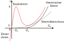
In the picture you can see that the diode in the area represents a negative differential resistance ; that is, in this area an increasing voltage leads to a decreasing current strength instead of - as in all common materials - to an increasing current strength. For example, a connected resonant circuit can be undamped ( oscillator ). It is therefore one of the active dynamic components.
Lambda diodes , which can be simulated by a simple electronic circuit consisting of JFETs , have a similar function, but with a larger operating range.
lifespan
Germanium tunnel diodes are very temperature-sensitive and, if soldered carelessly, can degrade to such an extent that they become inoperable. Both germanium and GaAs tunnel diodes are sensitive to overload. In particular, GaAs-TDs age within months to the point of uselessness if they are operated up to the range of the normal forward voltage with I p , even if the permissible power loss is not exceeded.
Rule of thumb for the limit for safe operation:
- I avg : Average operating current
- C j : junction capacitance
Applications
At very high frequencies, tunnel diodes can be used as amplifiers (up to a few 10 GHz), switches and oscillators (up to 100 GHz). This is due to the inertia-free quantum mechanical tunneling process, which can be seen in the current-voltage characteristic.
Superconducting tunnel diodes can be used as phonon emitters or phonon detectors.
See also
literature
- L. Esaki: New Phenomenon in Narrow Germanium pn Junctions , Phys. Rev. 109, pp. 603-604; doi : 10.1103 / PhysRev.109.603 .
- Nobel Prize speech by L. Esaki, Long journey into tunneling (PDF; 304 KB)
credentials
- ↑ Tunnel Diodes, Technical Manual TD-30 RCA, 1963, p. 29 ff.


