
Integrated circuit


An integrated circuit , and integrated circuit ( English integrated circuit , short IC , the letters are discussed separately: [ ʔiː ] [ TSE ] or outdated IS ) is a large on a thin, usually a few millimeters wafer of semiconductor material deposited electronic circuit . It is sometimes referred to as solid-state circuit or monolithic circuit ( English solid-state circuit or monolithic integrated circuit called). This chip ( english The ) is mostly to protect and simpler contact in a multiple larger chip package encapsulated. An IC typically contains a combination of numerous electrically connected electronic semiconductor components such as transistors , diodes and / or other active and passive components .
Integrated circuits can nowadays comprise circuits with many billions of electronic components (in particular transistors), so that even highly complex circuits such as microprocessors and memory chips can be accommodated on semiconductor wafers a few square millimeters . The microstructures of these elements have been manufactured in the nanometer range since the early 1990s . The rectangular semiconductor chips are chip (also called already in the green state), in particular together with the applied electronic circuit also microchip . ICs are manufactured in our own semiconductor factories in absolutely dust-free clean rooms and encompass a large number of process steps of a physical and chemical nature. As the performance of microprocessors and memory chips generally increases with smaller structures on the chip, their miniaturization is often at the limit of what is technically and physically feasible. However, there are also numerous, especially standardized ICs such as logic modules and operational amplifiers , where this only plays a minor role - the logic chips of the widely used 74xx series , which have been manufactured since the 1970s, only contain a number of transistors in the one or two-digit range .
Use of language
Colloquially now microchip or chip partially with an IC equated, even though the chip is only the "inner workings" of a circuit, that is, the English as the designated semiconductor chip to the actual circuit thereon.
Integrated circuits are also double, triple or other multiple components (regardless of whether as a semiconductor component or tube), which are each in a common housing or glass bulbs such as double diodes , triodes , pentodes , double or Triple darlington transistors , etc. are located.
history

predecessor
Before the development of integrated circuits, there were active electronic components that were hard-wired together with several passive ones and shipped in one housing. One example were the electron and vacuum tubes 3NF and 2HF , developed in the mid-1920s - the former a triple tube , similar to the later double triode ECC83 . In contrast to the younger tube, both of the 1920s tubes had four or two resistors and two or one capacitor built into the inside of the tube, just like in an IC . This resulted in finished radio circuits - the 3NF as a basic circuit for local reception and amplification and the 2HF in addition to the optional remote reception, where only the external components for station selection , power supply and playback ( loudspeakers or headphones ) and the antenna had to be connected.
By the late 1950s, electronic circuits were built with discrete components; H. with individual transistors , diodes, etc., which have been put together on a printed circuit board to form a circuit, cf. Integration (technology) . In terms of size and service life, this was already a major breakthrough compared to the electron tubes competing at the time .
Even before the invention of the transistor, there were electronic components that integrated several functions in one component , in the form of multi-system tubes , composite tubes such as the 3NF , duo diodes or even multi-anode mercury vapor rectifiers that function as several controlled or uncontrolled rectifiers (a cathode and several anodes) combined. Transistors have decisive advantages over vacuum tubes, e.g. B. Lower power consumption and size. With the use of printed circuit boards and the resulting downsizing of products, this newer technology began to replace the early tube-based integrated systems. This trend intensified completely with the development and massive use of integrated circuits from the 1960s.
Jacobi patent
Little known is the "semiconductor amplifier " invented and patented by Werner Jacobi in 1949 , a circuit made up of five transistors on a semiconductor that serves as a carrier material. These form a three-stage amplifier circuit in the form of an integrated circuit. Two transistors are switched "overhead" and thus effect the impedance conversion between the transistor stages. Jacobi stated that hearing aids , for example , could be made small, light and cheap.
An immediate commercial use of his patent is not known. The formulation of the integration concept is in the publicized on May 15, 1952 application: "semiconductor amplifier, characterized in that a plurality of acting in different switching or amplifier stages electrode systems are placed on the semiconductor." That is, for example, the integration of multiple light-emitting diodes in a The basic idea of the housing goes back to Jacobi.
From Kilby and Noyce to today


The first integrated circuit (a flip-flop ) was developed by Jack Kilby in September 1958 . It consisted of two bipolar transistors that were attached to a germanium substrate and connected by gold wires. This hybrid circuit is thus a first example of the implementation of the already known transistor-transistor logic (TTL) on a circuit. It was a preliminary stage for the further development of TTL circuits towards smaller designs.
The first "monolithic", i.e. H. In July 1959 , Robert Noyce applied for a patent for an integrated circuit made of or in a single monocrystalline substrate . The decisive factor in Noyce's invention was the complete production of the components, including wiring, on a substrate. Photolithographic and diffusion processes, which Fairchild Semiconductor had recently developed for the manufacture of the first modern diffusion bipolar transistor, have already been used for production. Based on these technologies, among other things, the first microprocessors from three companies were presented almost simultaneously in 1970/71: the Intel 4004 , the Texas Instruments (TI) TMS 1000 and the Garrett AiResearch "Central Air Data Computer" (CADC).
The first integrated circuits in series production emerged in the early 1960s (especially at Texas Instruments and Fairchild Semiconductor ). They only consisted of up to a few dozen bipolar transistors ( English small-scale integration , SSI), typically in RTL technology . Over the years, however, the components have become ever smaller, passive components such as resistors have been integrated and the complexity of the integrated circuits has increased. This also increased the number of transistors per chip or per unit area; the number of transistors was the most important characteristic of ICs.
The arms industry and space travel were a stimulating factor for further development. Until the mid-1960s, the US government was the main buyer of integrated circuits. The aim was to miniaturize the technology in both areas. From 1965 the Gemini program was equipped with on-board computers based on ICs.
With medium-scale integration (MSI) there was space for a few hundred transistors, with large-scale integration (LSI) at the beginning of the 1970s, for several thousand transistors. This made it possible for the first time to integrate an entire main processor (CPU) as a so-called microprocessor on a chip, which greatly reduced the costs of computers . At the beginning of the 1980s, the very-large-scale integration ( VLSI ) followed with several hundred thousand transistors, by means of which memory chips ( RAM ) with a capacity of 256 KiBit and 1 MiBit could soon be produced. With this further development of the manufacturing technology, an increasing degree of design automation (see chip design ) of the design and the photomasks required for manufacturing went hand in hand, without which the development of more complex circuits was no longer possible.
In 2010 graphics processors contained up to three billion transistors (see Nvidia Tesla ), "normal" general purpose CPUs up to 1.17 billion transistors (Intel Core i7-980X). The Itanium 2 Tukwila consists of 2.05 billion transistors. Graphics processors have now reached transistor numbers of over eight billion transistors ( Nvidia GTX TitanX ). Even larger numbers are achieved with memory modules, but with less complexity of the entire chip.

Different ICs
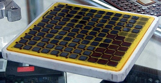
ICs on TCM ceramic carriers from an IBM mainframe
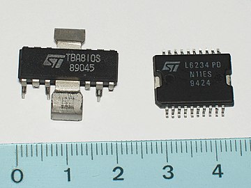
ICs in plastic housing
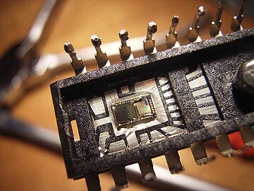
ICs in chip housing with connecting wires


Types and application

overview
The main feature of integrated circuits is a large number of different or identical active and passive components - the latter include resistors and capacitors - as well as connecting conductor tracks on or in a monocrystalline substrate. In this way they form the counterpart to circuits made up of individual (discrete) components soldered on a circuit board . Thick-film and thin-film circuits - whereby components are produced by vapor deposition and structuring of a thin layer on a glass substrate - and ( hybrid circuits ) occupy an intermediate position . There are a number of other distinctions:
According to the manufacturing technology
- monolithic circuits: all components are produced on a single piece (substrate) of monocrystalline semiconductor material ( chip ); The circuits are usually made by doping or epitaxy on the surface of the substrate material (diodes, transistors, up to a few micrometers above and below the original surface) or by applying layers (resistors, conductor tracks, capacitors, insulation, gates of MOSFETs , epitaxy) .
- Thin-film circuits are components that are produced by vapor deposition on a glass substrate. Most of them are resistance networks. They can also be manufactured with the highest accuracy by means of electron beam balancing. They are protected by dip painting. This group also includes circuits made of thin film transistors (TFT), such as those used in e.g. B. find application in flat screens.
- Thick-film hybrid circuits combine several monolithic chips as well as printed conductors and passive components (almost only resistors) in thick-film technology, mostly on a ceramic substrate; they are often dip-coated.
According to the type of signal
- Digital ICs process or store signals that are available in the form of a few discrete levels.
- Analog (linear) ICs process signals with any intermediate values.
- Mixed-signal ICs have both analog and digital circuit components.
Sensor and actuator ICs are converters between different physical quantities that are manufactured using microelectronic technologies. Examples are ICs in CMOS cameras , micromirror actuators , Hall probes , acceleration sensors or circuits for measuring their temperature, illuminance or for receiving digital infrared signals
After the task
- Processors are used as computing and control units for computers
- Semiconductor memories store digital data
- Miniaturized chips in the context of RFID technology for contactless identification of objects and living beings
- Standard logic ICs from various logic families offer functions across all applications
- ASICs are application-specific developments (e.g. in toasters, in vehicles, in washing machines)
- ASSPs are application-specific standard products that have special applications similar to ASICs, but are offered by the manufacturer and are not built at the customer's request
- Sensor ICs convert and process non-electrical quantities (e.g. acceleration, light, magnetic fields)
- DSPs (digital signal processors) process digital signals or analog signals in digital form
- D / A and A / D converters convert digital to analog values or vice versa
- FPGAs ( field programmable gate array ) are digital ICs that can be configured by the customer and consist of a large number of interconnectable functional units
- Microcontrollers (µC) contain all parts of a small computer (program memory, arithmetic unit, main memory and register)
- Power ICs can process high currents and voltages (e.g. as complete power amplifiers or in power supplies )
- System-on-a-Chip (SoC) are larger systems that are combined on one chip.
Manufacturing
overview
Integrated circuits are manufactured entirely on wafers ( monocrystalline semiconductor wafer), which is why one speaks of “monolithic production” or “monolithic integration”. On a 300 mm wafer between approx. 80 (with very large processors usually with a larger cache, e.g. Intel Tukwila ) and more than ten thousand (with individual transistors, simple circuits, LEDs, photodiodes, etc.), mostly identical integrated ones Circuits manufactured in parallel, which among other things reduces manufacturing costs. In addition to functional tests, the manufacturing process can be divided into three basic sections:
- The production of substrates, which includes the purification of the starting material, the production of large single crystals (so-called ingots ) and individual substrates (wafers)
- The manufacture of the individual components on a wafer, the so-called front end . This step can be divided into:
- Front-end-of-line (English front-end of line , FEOL, dt. ' Front end of the production line '): Here the (active) components such as transistors, diodes or capacitors are manufactured by processing the substrate material.
- Back-End-of-Line (engl. Back-end of line , BEOL, dt,. Trailing end of the production line '): This step involves essentially the so-called metallization, wherein the fabricated in the FEOL devices are connected to each other, and final passivation of the surface.
- The division of the wafers into individual chips and their packaging in housings, the so-called back-end (not to be confused with back-end-of-line ).
A "hybrid integration" (hybrid technology) - a combination of components made of different materials and manufacturing processes, such as thin and thick film technology - as used in the manufacture of microsystems, among other things, has so far not been used in the manufacture of integrated circuits. A comparable structure, 3D integration , in which several chips are stacked on top of one another and electrically connected to one another, could, however, be used in future ICs, cf. Multi-chip module .
Substrate production

The base material (substrate) usually serves both as a carrier and as a base material for the active areas of diodes and transistors. More than 99 percent of integrated circuits use silicon as a substrate material. Other materials such as gallium arsenide are also used for very high-frequency or optical applications . For special applications, silicon-on-insulator substrates (SOI substrates) or silicon on the insulating substrate such as sapphire ( silicon-on-sapphire , SOS) are used.
So that the high requirements of microelectronics can be met, the substrate must be manufactured in the form of high-purity single crystals . In the case of silicon, a monocrystalline cylinder ( ingot ) is first drawn from a high-purity silicon melt (cf. extraction of pure silicon ). The so-called Czochralski method (CZ method) is primarily used for this purpose. An alternative process is zone melting , which can also be used for further cleaning of the CZ ingots; For some special applications, higher degrees of purity are necessary than one foreign atom on 10 9 atoms of the CZ ingot. The ingots are cut into 0.5 to 1.5 mm thin slices, the so-called wafers . The silicon wafers used in mass production today (2016) have diameters of 150, 200 or 300 mm (also called 6, 8 or 12 inches), while wafers of 450 mm are still in the introductory phase. Through various etching, grinding and polishing processes, you get an almost perfectly flat surface with unevenness on the order of less than a nanometer, i.e. only a few atomic layers.
Front end

In the production of integrated circuits, all work steps before the wafer is diced are summarized under the term front-end ( i.e. front / first section ). It takes place in clean rooms with a very low density of dust particles. This is necessary because even the smallest particles (<0.1 µm ) can cause a complete circuit to fail. The processes and procedures used can be roughly divided into the following groups:
- Structuring processes (especially photolithography for structuring photoresist masks that cover areas on the wafer in the subsequent steps that are not to be treated (e.g. doped)),
- Process for layer structure ( epitaxy , sputter deposition , vapor deposition , CVD , etc.),
- Process layer removal and cleaning (dry and wet chemical etching processes) and
- Process for changing material properties (e.g. baking processes , doping , silicide formation ).
The front-end production is divided into two larger areas: the front-end-of-line (FEoL) and the back-end-of-line (BEoL). They differ both in terms of the functional elements to be manufactured and the manufacturing processes used in semiconductor technology and materials.
Starting from an unstructured wafer, the front-end-of-line essentially comprises all process steps for the production of the electrically active and passive components (transistors, capacitors and also resistors). In the back-end-of-line , however, the electrical connections between these components are made and only then linked to a functioning electronic circuit . In a figurative sense, wires, i.e. thin electrical lines made of metal, are manufactured and linked according to the circuit diagram. This is why one speaks of wiring or metallization.
The rough dividing line for the FEoL and the BEoL is the contacting of the transistor electrodes. The basic procedures used here correspond to a large extent to those in the BEoL. However, since special techniques and again different materials are used in this critical area, it cannot be clearly assigned to one of the areas. Therefore, the term middle-of-line has been established for this production section .
In the following, the essential process sequences for the production of modern, so-called metal-oxide-semiconductor field effect transistors (MOSFET) within larger integrated circuits are described in a simplified manner .
Front-end-of-line
The front-end production of a typical microprocessor starts with the production of the isolation areas between the individual components. Since the late 1990s, this so-called is largely grave insulation (Engl. Shallow trench isolation STI) used. Here first large grave areas in the substrate (usually silicon) etched . These areas are defined using a previously photolithographically structured resist mask, which protects the later active transistor areas from the etching attack. After the etching, the trenches are filled with an electrically insulating material (usually silicon dioxide), usually using chemical vapor deposition (CVD) processes. In order to ensure that no unfilled areas are created, significantly more dielectric material is deposited than is necessary. In order to obtain a smooth surface again, the excess material is removed by chemical-mechanical polishing (CMP) and the wafer surface is leveled.
Now the next manufacturing stage, producing the so-called "sinks" (in English follows wells ) and the preparation of the later transistor channel by doping the substrate material. The extrinsic electrical conductivity of the substrate material is changed locally. For example, doping a commonly used p-conducting silicon wafer (see also Czochralski method ) with boron creates an n-conducting trough in which the p-channel field effect transistors (FET), i.e. a transistor whose function is based on the Formation of an electrically p-conductive channel based, are produced. Well doping is necessary in order to be able to produce the two different variants of field effect transistors (n-channel and p-channel transistors) for the CMOS technology that has been used in integrated circuits for several decades . In addition, the pn junctions that arise during tub production help electrically decouple the differently doped areas. The simplest variant is the single-tub process already described (here for a p-tub). For certain requirements, however, a double (p- and n- well process ) or a triple-well process is also used. Nowadays, the doping itself is usually carried out by means of ion implantation over the entire surface of the wafer. In order to protect the areas that are to be or not doped differently, they are using a previously photolithographically patterned resist mask covered, it will be as usual by wet chemical processes after the processes of "structuring level '(z. B. piranha solution ) and / or plasma ashing removed. These same processes are also used for doping the transistor channel. In contrast to the wells, however, the doping is introduced close to the surface. Finally, there is usually a temperature process that heals the lattice defects that have arisen during the ion implantation and electrically activates the doping by installing it in the crystal lattice of the substrate.
The third process stage is used to build up the gate layer stack and the gate structuring. In the case of usual in the 1990s and 2000s CMOS process with silicon dioxide as the gate dielectric and polysilicon as the gate electrode, the very thin is first (a few nanometers thick) gate oxide produced, often through " Rapid Thermal Oxidation " (RTO, dt. About fast thermal oxidation ). This is followed by the full-surface deposition of a layer stack made of polysilicon and a thin encapsulation layer made of silicon dioxide. This oxide layer is structured by means of photolithography and etching. After removing the photoresist mask, the resulting structured layer serves as a hard mask for the gate structuring by means of an anisotropic dry etching process, reactive ion etching (RIE). In addition to trench isolation, gate structuring is one of the most demanding processes in FEoL. Especially the photolithography for the definition of the gate electrode still represents a technical limit for the miniaturization of the ( planar ) transistors. This is where highly specialized processes such as immersion lithography , reduction of the lines of the photoresist mask by an isotropic dry etching process ( resist shrink ) and Multiple structures are increasingly used. The already mentioned intermediate step is also a (relatively simple) special process, which is necessary because the photolithography, among other things, is unable to provide sufficiently thick photoresist masks of the necessary resolution that would withstand the etching process.
Simply put, the gate structuring is followed by the definition of the source and drain regions. In the case of older technology nodes (greater than 350 nm), this only comprised the special doping of the source and drain regions. For the LDD-MOSFETs (LDD = lightly doped drain ) typically used nowadays, however, this includes the doping of the drain extension ( extension implant ) and halo implants as well as the production of one or more spacers ( i.e. "spacers") ), via which the position of the dopants introduced by ion implantation can be controlled relatively easily. Only at the end does the final doping of the source and drain areas follow, with which the actual FEOL production section ends. Now the contacting and linking of the transistors begins.
Middle-of-line
After the actual transistor production, the individual components are connected. Before this happens, however, the transistor electrodes must first be electrically contacted. The contact manufacturing section is not clearly assigned to FEOL or BEOL, which is why this section is often referred to as Middle-of-Line (MOL).
In order to ensure good electrical contact between the semiconducting areas and the metallic connection (cf. Schottky contact ), the electrodes are first silicided , for example by the full-surface deposition of a nickel layer and subsequent silicide formation at high temperatures. After the silicide formation, the intermediate dielectric is usually deposited and leveled - mostly undoped silicate glass ( USG) or low-k dielectrics (increasingly since the mid-2000s). This is followed by the production of the contact holes using RIE and their filling with a metal, usually tungsten , which is deposited using a CVD process and leveled using CMP.
The stress layers used in some transistor technologies, which are intended to exert pressure or tension on the transistor channel and thus can influence the charge carrier mobility , are usually applied after the silicide formation and assigned to the MoL.
Back-end-of-line

The actual BEOL now follows the metallization, i.e. the production of a network of conductor tracks with which the individual components are connected. Typical materials are aluminum and, since the late 1990s, often copper. The production of the conductor tracks is heavily dependent on the metal used. In the case of aluminum, for example, the metal is first deposited over the entire surface and then structured using photolithography and a dry etching process . This method is not possible with copper, as there is no dry etching process for copper in which gaseous reaction products are formed. However, since the early 2000s there has been successful research into structuring copper in a high vacuum using dry etching processes. Instead, in the case of copper, the insulation layer deposited over the entire surface is first structured and then the copper is metallized using galvanic processes. Two main techniques are used here: the damascene and dual damascene process . They differ in the way in which the electrical connections, called VIA ( English vertical interconnect access ), are made between the actual conductor track levels (individually or together with the conductor track levels). The VIAs correspond to the plated-through holes on multilayer printed circuit boards . In the illustration it is the orange, vertical structures. In a finished integrated circuit there are then 13 to 15 such metallization levels one above the other. The structure size increases gradually in higher levels, for example the first two levels are manufactured in the smallest possible structure size (1 ×) and then follow two to five levels with a larger structure spacing (e.g. 2 ×) this can be up to 32- times (32 ×) coarser structures continue in the top level (intermediate levels can be omitted).
In addition to these conventional metallization there are other techniques such as silicon via ( English through-silicon via , TSV). It is currently used in some sensor applications that require certain functions on both the front and back of the chips, such as certain biosensors. However, it is also considered a promising technology for realizing a future 3D integration of integrated circuits. Several (heavily thinned) chips are stacked on top of one another and the individual chip levels are electrically connected to one another by TSVs. Since run in both cases, the TSVs through the wafer, it is also called wafer level through-silicon via (dt. Silicon via through the wafer ), see also ITRS in 2009.
In the case of some components, such as IGBT , the side opposite the circuit is additionally metallized in order to produce a conductive contact; however with only one or two metallization levels.
Back end
For use on a printed circuit board, the sensitive chip must be built into a housing .

In the so-called back-end , the wafers are divided into individual chips and these are usually placed in a housing.
Before dicing, the wafers are often thinned by grinding, known as "backlapping". The wafers are then only approx. 100 to 200 µm thick. The thinning is done to improve the cooling behavior of the chip. This is possible because in integrated circuits using thin-film technology, electrically active areas are only located in the first micrometers on the surface of the structure side. The remaining substrate material is only used for mechanical stability. The full substrate thickness is no longer necessary for sawn chips. However, thick substrates have a higher thermal resistance. Since the heat sinks are usually attached to the back of the substrate, thinned wafers have better cooling behavior.
The division of the wafers into the individual This is usually done by sawing, rarely also by scoring and breaking. So that the dies do not fall apart during sawing, the wafer is glued onto a sawing foil before sawing. Since the saw removes a piece from the wafer, the chips are not arranged seamlessly next to one another, but have a certain distance between them. In these tracks, the so-called “ scratch frames ”, test structures are also applied, which are used, among other things, for PCM measurements immediately after front-end production . These test structures are destroyed when sawing.

In the subsequent packaging (engl. Packaging ), the individual ICs are then introduced into a housing and contacted, the so-called bonding . Different processes are used depending on the type, for example chip bonding or wire bonding . Capping ( Einhausen ) is used for hermetic sealing against environmental influences - for purely electrical circuits must the housing gas and light tight to be - and to improve usability. Either the chip and bond wires are enclosed in a cavity (sheet metal, ceramic, possibly with a window) or encased with synthetic resin (cast, injection molding technique ). Highly complex circuits (mostly for mobile applications) have recently (2009) also been used without a base housing and soldered directly onto the respective circuit boards (cf. Ball Grid Array ). Finally, there is another function test, in which the guaranteed properties are checked on all circuits. The type test is carried out on a random basis or only in the development phase. The routine test is used to sort into circuits of different quality classes (for example according to offset voltage for operational amplifiers ) Test results and the type of capping determine the area of application. In this way, high qualities are produced for extended operating temperatures and environmental requirements (so-called MIL standard for military and space applications). Higher tolerances and plastic capping are possible for mass applications (consumer goods).
As a final step, the housing is printed with information from the manufacturer, e.g. B. with the manufacturer name, the type number, the date of manufacture u. In contrast to front-end production, back-end production is dominated by micromechanics and plastic processing methods ( injection molding ).
Function tests and process monitoring
In order to react to process fluctuations at an early stage, to correct faulty processes if necessary or even to remove wafers or lots from production, the still unfinished ICs are tested after many process steps. In the front end, these are mostly random samples in the form of a PCM test ( process control monitoring ). For the determination of technological parameters, the test (e.g. layer thickness test) is usually carried out directly after the respective process, here it is sometimes important to also record the respective systems, since identical systems with the same parameters produce deviations that can be outside the tolerance range. After the front end, all ICs are usually tested for their function before further processing. The most important electrical parameters of the components used are determined on special test structures that are located in the scratches between the chips. The parameters must comply with certain specifications in order to ensure that the chips work reliably in the entire permissible temperature range and over the full specified service life. In some cases, certain functions (RF circuits or connections of the chip that are later not connected to PINs) can only be tested on the die. Above all, for reasons of cost it must be prevented that non-functional ICs are further processed in the subsequent manufacturing process.
Although these measurements run fully automatically on special test systems ( Automatic Test Equipment ), the costs associated with highly integrated processor chips have almost reached the production costs. This is mainly due to the fact that economies of scale only take effect to a limited extent during testing (for example, parallelization is only possible with pure digital circuits) and newer ICs contain more and more functions that have to be tested one after the other. In order to be able to resolve the fine structures of microelectronics, rigid needle adapters are used nowadays , with which a measuring point distance of 150 µm can be resolved. Because of the precise guidance of the rigid needles, contact points with a diameter of 70 µm can be picked up and checked with such adapters. The rigid needle adapter also enables the contacting of fine-pole micro-plugs, which are being used more and more in microelectronics these days. This means that such plugs no longer have to be contacted with the rapidly worn mating connector. A learning curve is passed through with all new FE technologies. a. can be measured by the yield of functioning building blocks. Since a new FE technology involves considerable development costs (sometimes three-digit million amounts), companies have economic advantages that achieve high yield values as quickly as possible.
Finally, the packaged chip is also subjected to a final test before delivery in order to identify errors in the back-end production. Some properties are also tested that change due to the packaging or whose measurement is not possible without the housing, such as: B. the bonding or certain high frequency properties. The packaged chip can then go to the PCB assembly.
Miniaturization
Integrated circuits are seen as a separate electronic component. The size of the IC substrate (English which ) is as a rule only a few square millimeters , and is considerably smaller than the surrounding housing, which the actual electrical connections (pins) in manageable size for soldering holds. In order to keep the production costs of the often complex and costly ICs as low as possible, several (hundred to thousand) integrated circuits are produced in parallel on so-called wafers in microelectronics , but the production tolerances and errors that occur prevent a hundred percent yield.
In order to keep production costs as constant as possible or even reduce them in subsequent generations of more complex ICs, two major trends are being implemented in microelectronics. On the one hand, the chip area for the individual IC is kept as small as possible (main trend), on the other hand, as many ICs as possible are housed on a wafer, while the housing takes into account other requirements (soldering technology, heat dissipation, etc.) and, depending on market requirements, also shows different characteristics .
Keeping the chip area as constant as possible results in increasingly complex circuits - modern integrated circuits such. B. memory modules and microprocessors can contain billions of components (especially transistors) - the individual components such as transistors must be made smaller, which also enables a higher clock rate and a reduced operating voltage and therefore power consumption. With a constant chip area, however, costs can hardly be saved through higher parallelism in production. Therefore, the standard wafer size in production has been increased from 2-inch wafers to today's 12-inch wafers (actual diameter 300 mm). With the increasing wafer size, a more efficient use of the wafer surface went hand in hand (less waste). However, in order not only to keep the production quality the same, but to improve it - which was necessary due to the small components - major challenges in coating technology had to be overcome.
In general, miniaturization of the circuits will achieve the following objectives:
- One goal is a more efficient production, this is achieved, among other things, by parallel production on a substrate (English wafer ) and thus the saving of raw materials in production and further processing.
- Furthermore, the components should be more efficient in operation, so the reduction of the structures enables an increase in the switching speeds, this is achieved, for example, by shorter cable lengths and thus shorter signal transit times and lower latency times when reloading the capacities in the components, and by reducing the power consumption of the ICs.
- By integrating further functions, new ICs can often combine the functionality of several previously discrete ICs, which can also increase reliability, which is an important advantage over conventional, soldered circuits, especially in the initial phase of integrated circuits.
In this way, smaller, more power-saving components with more and more functions are to be produced, which is particularly important for mobile devices. The integrated circuits and their miniaturization enable telephone , SIM , money and credit cards, RFID , intelligent sensors, smaller and more durable pacemakers or hearing aids as well as MP3 players or CMOS cameras , etc. a. in cell phones.
Areas of application
Integrated circuits form the basis of all complex electronics today, especially computer technology. Only through integration is it possible to provide extensive functionality in a small space. In addition, in many cases , integrated circuits enable the technical implementation of systems that would otherwise be too expensive, too complex, too power-intensive, too large or in principle not feasible.
See also
- Common centroid layout
- Integrated optics
- Degree of integration
- Moore's Law
- Robert Widlar , Gordon Moore , Marcian Edward Hoff
- Property right for semiconductor topography (in Austria)
Web links
- Pioneers in IC development at heise.de
- Data sheets for various microchips at datasheetcatalog.com (English)
Individual evidence
- ^ Proceedings of Crack Paths (CP 2009) . University of Padua, Padua 2009, ISBN 978-88-95940-28-1 , p. 887.
- ^ History of Wireless . John Wiley & Sons, New Jersey 2006, ISBN 0-471-71814-9 , pp. 339 ff.
- ↑ Otto Stürner: The electron tube. In: radio technology. (= Göschen Collection. Volume V). Verlag Walter de Gruyter, Berlin 1927, p. 68 ff.
- ↑ Patent DE833366 : semiconductor amplifier . Registered on April 15, 1949 , published on June 30, 1952 , applicant: SIEMENS AG, inventor: W. Jacobi.
- ^ A b Jack S. Kilby: Invention of the integrated circuit . In: IEEE Transactions on Electron Devices . tape 23 , no. 7 , 1976, p. 648-654 .
- ↑ Patent US2981877 : Semiconductor device and lead structure. Filed July 30, 1959 , published April 25, 1961 , inventor: Robert N. Noyce.
- ↑ IM Ross: The invention of the transistor . In: Proceedings of the IEEE . tape 86 , no. 1 , 1998, p. 7-28 .
- ^ RG Arns: The other transistor: early history of the metal-oxide-semiconductor field-effect transistor . In: Engineering Science and Education Journal . tape 7 , no. 5 , 1998, pp. 233-240 .
- ^ David C. Mowery, Nathan Rosenberg: Postwar federal investment. In: Technology and the Pursuit of Economic Growth. Cambridge University Press, Cambridge (England) 1989, ISBN 0-521-38936-4 , pp. 145 f.
- ^ Robert Slater: Making the computer smaller and more powerfull. In: Portraits in Silicon. The Massachusetts Institute of Technology, Cambridge MA 1987, ISBN 0-262-69131-0 , p. 159.
- ↑ Nvidia: High-end graphics card GeForce GTX Titan X for $ 1000. In: heise online. Retrieved November 1, 2016 .
- ↑ V. Ney: light-induced dry etching of copper and cobalt with chlorine . Ed .: Free University of Berlin, Department of Physics. Berlin May 2004, p. 158 ( fu-berlin.de [PDF]).
- ^ Graphene. Semiconductor Manufacturing & Design Community, accessed February 10, 2017 (American English).
- ↑ Wafer Level Through Silicon Via (TSV) for 3D integration . In: International Technology Roadmap for Semiconductors 2009 Edition. Assembly and Packaging . 2009, p. 18–19 ( itrs.net [PDF]). itrs.net ( Memento from October 9, 2010 in the Internet Archive )