
Operational amplifier


An operational amplifier (abbr. OP , OPV , OPA, OpAmp, more rarely OpVer , OV , OA ) is an electronic component . It is a DC coupled amplifier with a very high gain. The name refers to the earlier use in analog computers and goes back to the mathematical term of the operator or the arithmetic operation . In addition to addition / subtraction, this also includes more complex functions such as differentiation, integration or logarithmization. Such operations are implemented by the external circuitry of the operational amplifier and are based on electrical voltages and currents . Operational amplifiers are versatile. The basic circuit of the operational amplifier is the differential amplifier . The actual function is determined by the external wiring .
The ideal operational amplifier is not feasible and can only be approximated in practice. This results in the need for a large number and range of available operational amplifiers, which differ in their properties and limit values. The most common feature are inputs with high impedance , the voltage difference of which is amplified on an output with low impedance. This output signal is related to a ground reference, which is usually not explicitly shown in the circuit diagram .
Operational amplifiers have established themselves as common components in electronics and, as an integrated circuit, are very small and inexpensive to manufacture.
The normal operational amplifier is a voltage amplifier with which a differential input voltage is amplified to a voltage output referenced to ground. But there are also other variants with different impedances of the connections and / or a different number of inputs and outputs. In order to differentiate the normal operational amplifier from other variants, it is often called VFA ( Voltage Feedback Amplifier ), but other nomenclatures are also used, such as VV-OPV according to Tietze-Schenk.
In circuit theory , the ideal operational amplifier can be modeled by a nullor . This means that the behavior of a circuit is only determined by the external wiring, the feedback network . This is expressed in the “golden rules of the VFA”: There is no current flowing through the inputs and the output of the counter-coupled OP tries to bring the voltage difference between the two inputs to 0 volts . This makes the analysis or synthesis of the circuit particularly easy, but it only maps the real situation to the extent that the real operational amplifier corresponds to the ideal.
history
The first differential amplifiers were built around 1930 with electron tubes. Together with the feedback theory of Harold S. Black and the work of Harry Nyquist and Hendrik Wade Bode , the essential fundamentals for operational amplifiers were in place at the beginning of the Second World War. These were initially developed in Bell Labs for defense applications, such as the M9 gun director system . The inventor of the operational amplifier is the Bell Labs researcher Karl D. Swartzel Jr., who applied for a patent for a summing amplifier in the United States on May 1, 1941 .
It received its English name " Operational Amplifier " in 1947 from John Ragazzini ; the German term "operational amplifier" is derived from it.
The development after the Second World War was towards finished modules, initially on a tube basis, such as the Philbrick model K2-W , which was developed in 1952 by George A. Philbrick Researches Inc. (GAP / R). This module was the first commercially marketed operational amplifier, priced at $ 20 at the time, and consisted of two 12AX7 electron tubes . These tubes, dual triodes , required a supply voltage of ± 300 V at 4.5 mA and allowed the output to be controlled by ± 50 V. At that time, GAP / R also published many technical application documents on the subject, such as the company publication Application Manual for Operational Amplifier for Modeling, Measuring, Manipulating, and Much Else , which highlighted many possible applications and contributed significantly to the widespread use of operational amplifiers. The circuit symbol still used today for the operational amplifier comes from GAP / R.
When suitable transistors became available at the end of the 1950s, significantly smaller and more energy-efficient modules were developed on their basis, e.g. B. P65 and P45 from GAP / R. These modules used discrete germanium transistors , the P45 was already implemented on a printed circuit board . A further reduction in size was made possible by the hybrid construction , in which the unpackaged transistor chips were mounted on a ceramic substrate together with other components. An example of this is the HOS-050 from Analog Devices , which was provided with a TO-8 metal housing.
With the development of silicon as a semiconductor material and integrated circuits , it became possible to manufacture a complete operational amplifier on a chip. Robert Widlar developed the µA702 at Fairchild Semiconductor in 1962 and the µA709 in 1965 , which was widely used. After Widlar left, Dave Fullagar at Fairchild in 1968 developed the successor µA741 with improved data and stability. The type 741 is the best-known operational amplifier and is still in production today under various names such as LM741 , AD741 or TL741 by various companies with the well-known number sequence "741".
Later on, the flat housings also became established for operational amplifiers: DIL housings with 8 or more pins (more if several opamps are combined in one housing) were used for small outputs, and housings with cooling surfaces for higher outputs. Soon the housings became even smaller, e.g. B. SOT 23-5, a plastic case only 3 mm in size with five connections.
The first current negative feedback operational amplifier was developed by David Nelson at what was then Comlinear (was taken over by National Semiconductor and is now part of Texas Instruments ) and initially sold in hybrid construction under the designation CLC103 . Comlinear and Elantec offered operational amplifiers with negative current feedback as integrated circuits from 1987 onwards.
Operational amplifiers have been further improved in terms of their mechanical and electrical properties and optimized for many applications in analog circuit technology . Depending on the requirements, different types of transistors such as bipolar transistors , JFETs and MOSFETs are used. As the number of units increased, so did the price of the components. Cross- manufacturer types, such as the quadruple operational amplifier LM324, are available for a few cents.

Operational amplifier K2-W with two double triode tubes

P45 (GAP / R): Discretely built operational amplifier from 1961

OPV 741 from 1979 in a TO-5 metal housing

Double OPV in a SO8 housing , type LM358


Structure and variants
There are different types of operational amplifiers, which are e.g. B. differ from each other by their low or high resistance inputs and outputs. The non-inverting (positive) input is almost always designed as a high-resistance voltage input. The inverting (negative) input is either a high-resistance voltage input or a low-resistance current input, depending on the type. The type of output can also be designed either as a low-resistance voltage output or as a high-resistance current output. This results in a total of four different circuit configurations, as shown in the following table.
Voltage output Current output Voltage input Normal operational amplifier
VV-OPV (VFA)
U a = A D U D
Transconductance amplifier
VC-OPV (English OTA)
I a = S D U D
Electricity input Transimpedance amplifier
CV-OPV (engl. CFA)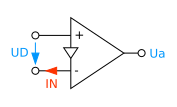
U a = I N Z = A D U D
Current amplifier
CC-OPV (English non-uniform)
I a = k l I N = S D U D


Other configurations are possible, but not common. So z. B. Schmid on 9 different variants. Such exceptions will not be dealt with further here; here we limit ourselves to the four practically significant variants, of which the VV-OPV variant dominates by far.
There are also fully symmetrical OPs that are equipped with two outputs, between which the output voltage is output differentially. In this case there is often a third input, via which the rest position of the output voltage is selected.
Conventional operational amplifier (VV-OP)
With conventional operational amplifiers or VV-OP ( voltage feedback OpAmp ), both inputs are high-resistance voltage inputs and the output behaves like a voltage source with the lowest possible resistance . In the early days of operational amplifiers, there was only this type and this class is still the most widespread today. Also in this article mostly only this type of operational amplifier is referenced. The advantages are its low offset voltage and high precision at low frequencies. The stability problems are disadvantageous, especially with capacitive loads in dynamic operation. Typical representatives of this class are the ancestor µA741 or the OP177 from Analog Devices .

Integrated operational amplifiers consist of a large number of different stages and circuit parts in order to be able to meet various requirements. Nevertheless, all these different variants can essentially be reduced to three circuit parts, as shown in the adjacent figure:
- A differential input, shown as a yellow area in the circuit diagram. This part consists of a differential amplifier with the two inputs, shown in the upper area, and a constant current source in the lower area. The differential amplifier converts a small voltage difference into a proportional output current. In a conventional operational amplifier, this stage also ensures the high input resistance . The input transistors can be bipolar transistors , MOSFETs or JFETs , depending on the technology . The different transistor types affect the size of the noise , among other things .
- An amplifier stage, highlighted in orange, which converts the small input current from the input stage into a high output voltage. The high straight gain of the operational amplifier results mainly from this stage. The capacitor drawn in the stage for internal frequency-dependent negative feedback is used for frequency compensation and thus guarantees the stability of the operational amplifier with an external negative feedback. Some ORs are externally frequency compensated, i. that is, the capacitor is not on-chip and can instead be connected externally. The housing has additional connections for this.
- One output stage, highlighted in blue. This level is often referred to as push-pull stage (Engl. Push-pull ) realized and, in contrast to the two previous stages no voltage gain. However, there are also OPs with amplifying output stages that are designed as open-collector or open-drain output stages and additionally require an external pull-up or pull-down resistor. The output stage usually serves as a current driver for the output, has a small output resistance and thus enables a high output current.
The small signal behavior of this circuit describes the equation
- ,

where U d symbolizes the input voltage difference , U a the output voltage, A 0 the straight-ahead amplification at low frequencies and GBP the amplification bandwidth product . ω C denotes the angular frequency .
Internal structure (internal circuit) of the µA741

In order to show the complexity of real operational amplifiers in comparison to the simplified model, the internal circuit of the well-known µA741 is shown below. This integrated circuit (IC) was developed in 1968 and reflects the state of the art at that time. It was widely used by the specialist journals to introduce the then new technology of operational amplifiers and in circuit proposals. So it initially became the best known and most widely used operational amplifier with almost no alternative. Today it is still produced in small numbers, primarily for replacement needs.
The area with a blue border on the left represents the input stage (differential amplifier) with constant current source. Additional connections are made in this stage to adjust manufacturing-related errors (offset errors), to which a potentiometer can be connected for fine adjustment. The three areas outlined in red represent current mirrors for the various stages . Current mirrors are current-controlled current sources and in this case are used to supply the amplifier stages.
The area outlined in magenta is the primary voltage amplifier stage , consisting of a Darlington pair with two transistors. The area outlined in green creates a bias voltage for the output stage outlined in turquoise on the right. The 30 pF capacitor drawn in the middle is used for frequency compensation . The production of this capacitor directly on the silicon chip was a major innovation in semiconductor production at the time.
Current feedback operational amplifier (CV-OP)

In the current feedback operational amplifier , abbreviated CV-OP ( current / voltage-OP ) or CFA ( current feedback amplifier ), the inverted input is a low-resistance current input and the output is a voltage source with the lowest possible resistance. One advantage is its high bandwidth , which allows it to be used as a video amplifier, for example. A disadvantage is a relatively high offset voltage. A typical representative of this class is the CLC449 component from National Semiconductor .
The figure opposite shows the simple internal circuitry of a current-fed operational amplifier. In contrast to the conventional operational amplifiers with voltage inputs shown in the previous chapters, the low-resistance current input in the input stage with a yellow background is connected directly to the emitters of the input transistors. The orange highlighted amplifier stage in the middle consists of two current mirrors that control the push-pull output stage highlighted in blue. The small-signal behavior results in what, together with the negative feedback network, considered as a voltage source with the output resistance , leads to: The forward gain can be controlled by the impedance of the negative feedback network, the lower the impedance, the greater the forward gain.


Transconductance operational amplifier (VC-OP)
In the case of the transconductance operational amplifier or VC-OP ( operational transconductance amplifier , abbreviated to OTA), both inputs are high-resistance and the output behaves like a high-resistance current source , the current of which is controlled by the voltage difference at the inputs. One of its advantages - in addition to the low offset voltage - is the ability to drive capacitive loads dynamically. The disadvantage is that the load must be known when dimensioning the circuit. A component from this class is the LM13700 from National Semiconductor .
Current amplifier (CC-OP)
The current amplifier or CC-OP, also known under the brand name English diamond transistor , has a low-impedance and inverted current input and a current output with the highest possible impedance. This type of operational amplifier behaves almost like an ideal bipolar transistor, with the exception of the current direction at the collector. The base functions as the high-impedance non-inverting input, the emitter as the low-impedance inverting input, and the collector as the high-impedance output. In contrast to a real bipolar transistor, the currents can flow in both directions, i.e. H. There is no need to differentiate between NPN and PNP, one component covers both polarities.
In contrast to real bipolar transistors, the CC-OP requires a power supply and, like other operational amplifiers, is not a 3-pole component. The currents to the emitter and collector are in the same direction, that is, they both go into the component, or both go out. The sum of both currents flows through the operating voltage connections in addition to the quiescent current. In the Sedra / Smith classification, it is a CCII + ( Current Conveyor , second generation, positive polarity). The real bipolar transistor, on the other hand, would be an implementation of the CCII-.
A representative of this class is the OPA860 from Texas Instruments . This also contains an impedance converter (voltage follower), with the help of which you can turn the output into a low-impedance voltage output, resulting in a CFA. The impedance converter can, however, also be connected upstream of the "emitter", which makes it high-impedance. That makes an OTA. Three different configurations can be implemented with one component. For this reason, the component is also marketed as an OTA, but it can also be operated in the other configurations. The relationship to the CFA can be seen in the schematic diagram of the CFA shown: The part with a blue background is an impedance converter. If it is removed, you get a CC-OP. The impedance converter is available in the OPA860, but its connections are led out separately so that the user is free to use it.
function
OPs are designed for use with an external feedback network that defines the function. As a rule, the negative feedback dominates , because otherwise only the highest or lowest possible output voltage is present at the output due to the size of the amplification factor of the OP, and thus the "linear" range would be left, in which the golden rules apply. Most OP applications keep it in this linear range through negative feedback. The OP controls the output to the voltage that causes the negative input to be equal to the positive input, i.e. the differential input voltage is 0.
However, there are also some applications that deliberately leave the linear range. The output then assumes either its minimum or its maximum voltage, so it only knows two states. This “ digital ” operating mode ( comparator ) is the result of renouncing negative feedback due to the high gain. In the case of positive feedback , there is a hysteresis as with the Schmitt trigger . The suitability of an OP for this operating mode must be checked, because the associated input voltage difference is outside the permissible range for some OPs.
The negative feedback required for linear operation reduces the overall gain of the circuit, consisting of the operational amplifier and feedback network, and defines an exact (practically only dependent on the accuracy of the components of the feedback) operating behavior of the entire circuit (see negative feedback for a list of the associated advantages ).
The wiring of the operational amplifier allows very different functions to be implemented. With just a few resistors, circuits can be set up that add, subtract or multiply voltages as an analog value or by a fixed factor. More complex functions are possible with capacitors. Analog filters or the closely related mathematical functions such as integration and differentiation can be implemented in this way .


The basic formula for the operational amplifier component is

with = open circuit voltage gain. Almost always the best permissible approximations lead to the "ideal operational amplifier":

Use without feedback as a comparator
- Without feedback from the output on the inputs, it can only have two values:
- positive overdriven if
- negatively overdriven if .
- (The mathematically exact singular point cannot be physically realized.)


Use with feedback to the inverting input
- The circuit can be operated using analog technology without overloading. This must be set because the output is not overdriven .


Example: In the simple diagram opposite, the output acts with an ohmic resistor back on the input marked with a "-". Because of this , the entire input current flows through the resistor. A positive input current pulls the input into the positive, which makes it even more so . The influence of the input side counteracts via the resistance. The current is drawn from the amplifier output with such a large negative that it is what is achieved at .


Note: does not apply in mathematical rigor. The tension is insignificantly small, but it must be so great that it can have a sign.

Examples of feasible operations
The operational amplifier has a wide range of possible applications, for example in various amplifier stages such as preamplifiers and measuring transducers , as well as in analog filters , analog-digital converters and in stages for analog signal processing .
In the following simple circuits, which form the basis of many applications of the operational amplifier, an ideal, voltage-controlled operational amplifier is always assumed for reasons of clarity. The implemented operation is only determined by the external wiring. The two inputs provide a choice of which of the inputs the input variable should act on. With the feedback, so that it becomes a stabilizing negative feedback, there is no option.
In these examples, two voltage sources are required for the supply, one with positive and one with negative voltage with respect to the reference potential ground , so that the operational amplifier can generate positive and negative output voltages and currents.
Action on the non-inverting input
Voltage follower

The circuit called a voltage follower is a variant of the non-inverting (linear) amplifier. The inverting input is directly connected to the output. The negative feedback causes the voltage difference between the two inputs to be zero. That gives the connection

and a gain factor . The voltage at the output follows the voltage at the input unchanged, from which the name voltage follower is derived.

The input resistance of the circuit results approximately from the input resistance of the operational amplifier , the open circuit voltage gain of the operational amplifier and the gain of the circuit


- .

The voltage follower has the lowest possible gain and the highest possible input resistance of all non-inverting amplifiers. Conversely, the approximation applies to the output resistance of the circuit

- ,

so that it is as small as possible. The voltage follower is therefore particularly suitable as an impedance converter , which almost does not load a voltage source, but can itself be loaded.
Non-inverting amplifier (electrometer amplifier)

With this amplifier, a voltage divider consisting of two resistors is switched into negative feedback opposite the voltage follower . Only the falling part of the output voltage is fed back to the inverting input. The differential voltage between its inputs is kept at zero, for which purpose the output voltage is always greater than the input voltage. Since the voltage divider is not loaded by any branching current, the gain factor results directly from the ratio of total resistance to partial resistance:


This leads to the output voltage :

On the input side, the amplifier "measures" the input voltage without the amplifier, acting as a voltmeter, loading the voltage source with a current - like an electrometer . On the output side, the amplifier behaves like an ideal voltage source . The functional equation applies to a connected load regardless of the output current required - up to the limit of the operational amplifier's ability to deliver.
The smallest gain that is possible with this circuit is . It arises when or is, whereby the circuit becomes a voltage follower . The situation is different for the smallest gain in the inverting amplifier .


Voltage-current converter

Such circuits can be found, for example, in industrial measurement technology, since current signals can usually be transmitted more easily with fewer errors than voltage signals (e.g. standard signal 4 to 20 mA). The measuring resistor acts as a proportionality factor and should have a tight tolerance. In the adjacent circuit, the current through the load resistor is set in such a way that the voltage is generated:


- ,

where this current is independent of . The size of is limited by the fact that the operational amplifier is limited in its output voltage. This circuit has the disadvantage that the load resistor must be potential-free to ground. Further circuit variants with which this disadvantage can be avoided are described for the constant current source.
Action on the inverting input
Inverting amplifier

As a result of the negative feedback, the operational amplifier controls its output in such a way that the differential voltage between its inputs is kept at zero. In the specified circuit with the non-inverting input connected to ground, it can therefore be assumed that ground potential is also established at the inverting input (-), but without being connected to ground by wiring. This junction is also known in technical terms as the virtual mass . The resistance then lies between the input terminal and ground, and lies between the output terminal and ground. Since it can furthermore be assumed that no current flows into the inverting input, all of the current that occurs in must also flow into; A voltage must appear at the output that is as large as the voltage drop that occurs with this current on :


The gain factor is negative. In the case of direct voltage, this means a change in sign between the input and output voltage; in the case of sinusoidal alternating voltage, a phase shift of 180 °. The input resistance , which is loaded, is not derived from a property of the operational amplifier, but from the design of the circuit: It is identical to .

If and are equal, the input voltage at the output is shown with the opposite sign.
In the case of the inverting amplifier, amplification without additional components is also possible, which allows attenuation.

Inverting adder / summing amplifier

The circuit is closely related to the inverting amplifier, but this is expanded by at least one input.
The term adder has become common, although the sign of the sum is changed by the circuit. The input voltages are added up and amplified. From a physically strict point of view, it is currents that are added and then continue to flow in their sum . Due to the virtual ground potential, no current through one input influences the current through another input. There is an input resistor at each input, which allows the individual voltages to be added to be weighted differently. This circuit can be used with any number of inputs (summands).

The equation for the output voltage results for the circuit shown with three inputs as follows:

The input voltages can be positive or negative. If two voltages are to be subtracted, the voltage to be subtracted can be inverted via an amplifier and then added. Without this detour, there are subtractors that act on both inputs of the operational amplifier or as a circuit with several operational amplifiers .

Current-voltage converter

The current-voltage converter converts an input current into a proportional voltage . Since there is no voltage between the virtually and actually grounded inputs, there is no voltage drop in the input circuit in this circuit. For the closed circuit, the second pole of the power source must be connected to ground.
With the resistor as a proportionality factor, the ratio of input current to output voltage can be set:


The voltage that is needed to allow the input current to flow through the resistor is present at the output . The circuit can be used to process signals from power sources . It is also known as a transimpedance amplifier .
Current-current converter

The current-current converter maps an input current to an output current proportional to it. It can also be called a current amplifier. The resistors and form a current divider . Only the part of the output current flowing through is fed back to the inverting input. the equation

applies regardless of the connected load resistance . On the input side, the converter "measures" the input current without the converter acting as an ammeter loading the current source with a voltage drop. On the output side, the converter behaves like an ideal power source . The functional equation applies to a connected load regardless of the output voltage required for this - up to the limit of the operational amplifier's controllability.
In the special case, if or is, this converter becomes, in terms of circuit theory, the counterpart to the voltage follower, a current follower, so to speak, but inverting:
- .

Integrator


An integrator is a circuit with a capacitor as negative feedback . With this component there is a dependence on time. The capacitor is an analog memory that is charged by the input current. This current arises due to the falling input voltage and generates an increase in the voltage on the capacitor with a rate of increase determined by the current.


If for and


if for , then is


With a constant positive, this results in a straight line with a negative slope. Without countermeasures, an integrator operated with DC voltage on the input side runs to the limit of its modulation range.
Integrators ensure a balancing behavior. They can also form function generators, for example to generate triangular waves from square-wave signals.
The picture on the right shows the temporal course of the input and output voltage, ideally free of any influence from a direct component on the input side. The peak-valley value of the output voltage is proportional to the period or inversely proportional to the angular frequency :


The larger the frequency, the smaller it becomes . Correspondingly, with a sinusoidal voltage, the amplitude is weakened with increasing frequency .
Mean value images


In the adjacent circuit , also known as a low-pass filter , the resistor takes over the feedback at low frequencies, if is ; the circuit behaves like an amplifier. In the opposite case, if is, the capacitor takes over the feedback and produces the behavior of an integrator. This means: the input voltage is amplified; for AC components contained therein but above a by and given frequency, the reactance of the capacitor takes place of the feedback, whereby these components are attenuated with increasing frequency. In summary, this gives the function equation


This active low-pass loads the signal source purely ohmically with the input resistance , i.e. regardless of the frequency.
In the case of a square-wave voltage, the fundamental frequency of which is low compared to the cut-off frequency of the low-pass filter, only the higher-frequency components that form the edges are weakened, which is shown in the figure in the upper curve of the output voltage by rounded edges.
At a much higher fundamental frequency, all alternating components are almost suppressed, and only the direct component determines the output voltage. This case is shown in the lower part of the picture, in which only a small influence of the alternating voltage is visible.
Differentiator

The differentiator has a capacitor between the input terminal and the virtual ground at the inverting input of the amplifier. Since one pole of the capacitor is held firmly at ground potential, the entire input voltage at the capacitor drops. A charge-reversal current flows in it proportional to the speed at which the input voltage changes. The output voltage becomes as great as the voltage drop across the resistor due to the current.


with the time constant . With DC voltage is .


The differentiator can also be viewed as a first-order high-pass filter : The capacitor at the input blocks the DC voltage; the higher the frequency for AC voltage, the lower the reactance of the capacitor. If it is viewed as the input resistance of an inverting amplifier, the gain increases the higher the frequency or the smaller the reactance (6 dB per octave or 20 dB per decade).
The circuit tends to overshoot with higher frequency components of the input signal. In order for it to be stable, a resistor is often connected in series with the capacitor. This limits the increase in gain associated with increasing frequency to the value as with ohmic wiring . This also prevents the output signal being too high or distorted in the event of voltage jumps.
In the control technology differentiating elements are used, in order to respond briefly disproportionately fast deviations.
Logarithmizer and exponentizer

The logarithm and the inverse function, the exponentiation , are non-linear functions that can be simulated with the characteristic of a diode . For this applies approximately in the forward direction

There are , and constants, which, however, depend on the temperature. In the adjacent circuit of the logarithmizer, a current flows proportionally with a positive input voltage , but the negative output voltage only increases logarithmically with the current:


In the next circuit, the current increases exponentially with the voltage at the diode, and the output voltage at the resistor increases accordingly.

Logarithmizers and exponentiators that are implemented in practice are more complex in construction and usually use bipolar transistors instead of diodes, which can reduce undesirable influences. They have temperature compensation. However, this does not change the underlying functional principle.
After logarithmizing, multiplications and divisions can be carried out using addition and subtraction. This means that two logarithmizers, followed by an adder or subtracter and a subsequent exponentiator, can be used as an analog multiplier or divider.
Applications are, for example, modulators , measuring devices that work without switching over several orders of magnitude , ratio pyrometers , rms meters .
Action on both entrances
Differential amplifier / subtracter amplifier

In the case of a differential amplifier or subtractor with an operational amplifier, it is wired in such a way that it works like an inverting and a non-inverting amplifier at the same time. A voltage divider acts on the non-inverting input of the operational amplifier; acts on the inverting input, which however is not virtually connected to ground. The output voltage is established according to the equation


- .

If the corresponding resistors in the circuit have the same values ( , ), the output voltage is the difference between the input voltages, multiplied by the ratio of :


For the factor in front of the brackets is equal to one:

- .

However, the relationships are not as simple as the equation shows. If resistance ratios are nominally the same, they will be summarized in the invoice and reduced if possible. The existing resistance ratios deviate from one another due to the variation in the resistances, and they also allow the transfer behavior to deviate from the ideal behavior, although they do not appear in the equation.
One application of such a circuit is the conversion of symmetrical signals to a ground-related signal. Interferences that affect both signals equally (common-mode interference) are eliminated. The prerequisite for this is that the ratios of the resistances are as exact as possible and that the internal resistance of the signal source is negligibly small. The input resistances of both signal inputs are the same for common-mode signals, which means that optimum common-mode rejection is achieved. For input signals that differ from one another, the input resistances are different: for the non- inverting input, its resistance is , for the inverting input, it is dependent on . The instrumentation amplifier described below avoids this possible source of error.


Circuit with several operational amplifiers
High input resistance subtracter

The following applies to the circuit shown

With and the equation is simplified to


If all resistors are made the same size, the circuit generates

A factor one in front of the bracket would also be conceivable, but is not possible with this circuit.

The previously mentioned problem with resistance ratios, which are not visible in the final equation, but are effective in the circuit, also applies here.
Instrumentation amplifier

The differential amplifier described above can be expanded to an instrumentation amplifier with two additional operational amplifiers . The instrumentation amplifier is also referred to as a measuring amplifier , instrumentation amplifier or electrometer subtractor and is mainly used to amplify measurement signals. It is available as an integrated circuit in which the aforementioned problem with imprecise resistance ratios can be reduced by adjustment in the manufacturing process.
In contrast to the differential amplifier, the instrumentation amplifier has two high-impedance inputs of the same type and higher common-mode rejection .

The gain can be set via a single resistor , which is why the connections of this resistor are brought out for individual assignment in integrated instrumentation amplifiers. If there is no (open terminal), the gain is one.
Rectifier

Silicon diodes have a very small reverse current on the one hand, and a considerable forward voltage on the other hand, which can have a very falsifying effect. In the precision rectifiers and peak value rectifier diode takes over (in the picture: D2), although the rectification, but their forward voltage is not included in the output signal of the rectifier circuit by instead is taken as the output voltage. The transfer function applies to the adjacent circuit


- .

Other uses
In addition to being used as active first-order filters, operational amplifiers can also be used to build higher-order filters. The Sallen-Key filter is an example of a particularly simple 2nd order filter with only one operational amplifier; different filter characteristics such as Butterworth or Chebyshev filters and functions such as low pass , high pass and band pass can be implemented. Other filters such as all-pass filters can also be built up with operational amplifiers. Higher filter orders are achieved by connecting several active filters in series.

Coils are difficult to accommodate on circuit boards . However, inductances can be simulated using an operational amplifier and capacitor. The notation with complex quantities applies to the circuit shown


This makes the circuit between the terminals appear like an inductive impedance

In general, operational amplifiers can be used to build impedance converters that can, for example, implement gyrators for simulating large inductances without the disadvantages of coils, as well as circulators for separating signal directions or negative impedance converters that behave like "negative resistances".
There are also versions with integrated power output stages, so that the output signal can be used, for example, to control actuators in controls or loudspeakers .
Calculation of operational amplifier circuits

To calculate operational amplifier circuits , it is useful to use an equivalent circuit diagram for the operational amplifier, which models the component with different, easier-to-use components.
Since an ideal operational amplifier is functionally a controlled voltage source , it can be replaced at the output by a controlled voltage source with the two differential inputs as a control voltage. This makes it possible to calculate the entire circuit using the node, mesh and superposition theorem . The control voltage is set to zero for ideal operational amplifiers because of the infinite straight-ahead gain. In the case of non-ideal operational amplifiers, a finite straight-ahead gain applies .


Example with an inverting amplifier


The superposition theorem gives for the differential voltage:

For the ideal operational amplifier with then follows:


For the properties of a real operational amplifier, further sources or resistors can now be added in order to better adapt the circuit model to the real conditions. For sensitive amplifiers, such as microphone preamplifiers , it is often necessary to take into account the leakage currents of the inputs and the offset voltage. The leakage currents I B are approximated with current sources, the offset voltage U Os as a voltage source in series with the two inputs, as shown in the following figure.
Properties of real operational amplifiers
The real operational amplifier tries to approximate the model of the ideal operational amplifier. Due to physical limits, such as a maximum supply voltage, but also manufacturing tolerances due to impurities in the semiconductor material , production fluctuations and the like, however, there are deviations from the ideal behavior. The corresponding restrictions are named in the data sheets; they provide important information for the correct and successful use of the component in a circuit. Circuit simulation programs such as SPICE model these restrictions in varying degrees of detail.
The significance of these restrictions varies depending on the requirements in a specific circuit. The requirements sometimes conflict with one another. Typically, the power consumption of low-noise types is greater, the less they noise. Even a high cut-off frequency is usually bought at the cost of a high power requirement. This opens up space for a large variety of types from which a user can choose the most suitable type.
The most important parameters include the parameters listed in the following subsections.
Power supply and current consumption
The ideal operational amplifier does not need any electricity and can generate output voltages of any size. In reality this is not possible; Restrictions apply to the power supply of the component. The supply voltage at which an operational amplifier will function and not be damaged depends on the manufacturing technology and the circuit design. The current consumption of the operational amplifier consists of the so-called quiescent current and the current consumption via the output. The quiescent current is used to operate the internal circuits of the operational amplifier and is approximately constant.
Early tube-based operating rooms operated with a symmetrical operating voltage of ± 300 V. Early integrated operating rooms such as e.g. B. the mentioned µA741 were designed for an operating voltage of ± 15 V; a power supply for operating theaters that is still widely used today. OPs for low operating voltages of 5 V and below are becoming increasingly important, following a general trend towards lower operating voltages.
In general, OPs can only generate output voltages that are within the range spanned by the operating voltages. How close you get to the operating voltages in practice depends on the specific internal design of the component. So-called “rail-to-rail” outputs make it possible to get very close to the operating voltages (rails), possibly even closer than 100 mV, depending on the output current. Other constructions need u. U. 2 V distance to the operating voltages, or even more. So-called. “Single-supply” OPs usually allow an approximation of the negative supply to values below 1 V, but not a corresponding approximation of the positive supply.
If the output voltage tries to leave the range supported by the OP and its power supply, because this is “required” by the feedback, then the gain collapses and the linear operating range is left. The above-mentioned “golden rules” then no longer apply.
The quiescent current of the OP can differ greatly between different models. Micropower OPs with quiescent currents below 1 µA are on the market. On the other hand, OPs for high power or high frequencies may need quiescent currents of over 100 mA.
In addition to the two operating voltage connections, early operational amplifiers also had a ground connection (e.g. the K2-W and the µA702). This is now unusual, because the operating voltage connections can also fulfill the function of the ground connection. There are only DC voltage differences between the operating voltage connections and the ground; for AC voltage they are all equivalent. It is therefore irrelevant for an OP whether the ground is in the middle of the operating voltage (symmetrical supply), whether it coincides with an operating voltage connection (usually the negative; single supply), or whether it is on a different DC voltage potential. The specification ± 15 V is therefore equivalent to the specification +30 V.
Common mode voltage ranges
Restrictions apply to both the output and the inputs with regard to the voltage range relative to the operating voltages in which the component works normally (in the linear range). The permitted range for the voltages at the inputs is English. Called "Input Common Mode Range". If it is left, the reinforcement collapses, with more drastic consequences depending on the component. In some models, the role of the inputs is reversed. If the supply voltage range is left, the component can be permanently damaged in many models.
Some models allow input voltages below the negative supply (usually a few 100 mV), other models allow voltages above the positive supply (also usually a few 100 mV). Types with “rail-to-rail” entrances allow both.
The same applies to the output, except that voltages outside the operating voltages are not supported. There are very few exceptions with built-in charge pumps for special areas of application.
Supply voltage feedthrough and common mode feedthrough
An ideal operational amplifier generates its output voltage without any external influence, e.g. B. from the power supply. Such an influence exists in real operating theaters. H. Small residues of a fault on the power supply can also be found in the output signal.
The effect of supply voltage variations on the output voltage as a power supply rejection ratio (English power supply rejection ratio PSRR) and referred well suppressed by a suitable design of the internal circuit as possible. Simple operational amplifiers achieve a PSRR of 70 dB.
There is also an influence of the common mode signal on the output voltage. A common mode signal is present at the input if the voltage at both inputs changes in parallel relative to ground. Since the OP should only amplify the difference between the inputs, the output should remain unaffected. In reality, there remains a slight influence, the size of which is specified in decibels as the common mode rejection ratio (CMRR).
Temperature range, housing and cooling

Integrated operational amplifiers are usually offered for an ambient temperature range from 0 ° C to 70 ° C down to −55 ° C to 125 ° C. In addition, there are special types for ambient temperatures of more than 200 ° C, for example, the quad operational amplifier HT1104 by Honeywell .
The power loss that occurs in the operating room heats the component internally beyond the ambient temperature. In addition to the limitation of the ambient temperature, there is therefore a limitation of the maximum chip temperature (more precisely: junction temperature, usually referred to as T J , limit often at 150 ° C) to avoid its damage. Possibly. the temperature increase must be estimated, for this purpose the manufacturer provides information about the thermal resistance between the chip and the environment, depending on the type of assembly. Depending on the power dissipation to be dissipated as heat, there are different housing shapes that allow different types of assembly, e.g. B. also on heat sinks .
It is common to offer several housing variants for an OR. This not only covers different cooling requirements, but also supports different assembly techniques and levels of miniaturization. The housing shapes that were dominant in the early days were intended for use in sockets, but today SMD soldering technology dominates . The relatively large and tinker-friendly DIL housings are still popular, but the smaller SMD housings are produced in significantly larger quantities. Newer OR models are often only available in small SMD housings. The smallest variants are hardly any larger than the silicon chip itself.
Output impedance and current
The output resistance of an ideal OP is 0 with a voltage output and infinite with a current output. The output voltage and output current are unlimited. That is not achievable in reality.
The output stage of an operational amplifier has a current-voltage characteristic curve, which can be approximated by a differential resistance , the output resistance . This reduces the controllability of the output according to Ohm's law , depending on the output current. Within these limits, the output resistance can usually be neglected due to the negative feedback; an exception is a capacitive load on the output, which forms an RC element or a low-pass filter within the negative feedback. The resulting phase shift can lead to instability of the entire circuit.
The maximum output current is usually a few 10 mA, the output is normally short-circuit proof. In addition, there are special integrated operational amplifiers that can deliver output currents of up to 10 A. These are installed in suitable housings that can dissipate the heat losses associated with the high currents. Alternatively, external complementary transistor collector stages can also increase the load current of an OP.
Input impedance
The voltage inputs of an ideal OP have an infinite input impedance. In the case of current inputs, it is 0. This cannot be achieved in reality.
All OPs have parasitic input capacitances, mostly a few pF. These are particularly noticeable at higher frequencies.
The input resistances of a real operational amplifier can be divided into two groups:
- Common mode input resistors
- These two resistors are between the respective input and ground. They are therefore parallel to the inputs and are therefore not influenced by negative feedback. The common mode resistance at the non-inverting input causes a weakening, that at the inverting input increases the gain. When these resistances are balanced in the operational amplifier, their effects compensate each other completely. In real operational amplifiers there are slight deviations, but since the common-mode input resistances are generally very high, in the range of a few 10 MΩ upwards, their influence can usually be neglected.
- Differential input resistance
- This resistance lies between the non-inverting and the inverting input and has a strong dynamic effect due to negative feedback. By means of negative feedback with only finite common-mode rejection, the voltage between the two inputs is always kept close to zero volts, which means that dynamic resistance values in the range of a few 10 GΩ are typical.
Input currents
The golden rules require that no currents flow into the entrances. In practice, however, small parasitic currents flow, which differ greatly between the OR models.
The parasitic input currents correspond to the base or gate currents of the input transistors. The typical values for operational amplifiers with field effect transistors are a few pA at room temperature, but increase sharply with temperature. In the case of bipolar transistors, the input currents are typically in the range of 1 nA to 1 µA and are only slightly dependent on the temperature.
The input currents of the two inputs are of a similar magnitude, but not exactly the same. This is why the manufacturer's specifications usually specify the mean input bias current as well as the difference between the currents ( input offset current ).
The size of the error caused by the input currents is directly proportional to the choice of external wiring resistors. The higher the resistance dimensions, the greater the effect of the input currents as an error. With the same resistances and currents at both inputs, the errors can largely cancel each other out.
Offset voltage
The offset voltage is a characteristic of operational amplifiers as a result of systematic errors in a circuit. It is the difference between the input voltages when the output voltage is 0 V.
The production-related offset voltages are typically in the range from 1 to 10 mV. With certain types, for example the OP27 , the offset voltage is lowered by adjustment during manufacture to the range of 10 µV and below; these mostly also have a low temperature dependence of typically less than 1 µV / K. A further reduction of up to 1 µV is possible using a so-called chopper stabilization , in which the offset voltage is measured and compensated for during operation; this also largely eliminates the temperature drift of the offset voltage.
Noise
The noise of operational amplifiers can be described by specifying a noise voltage density and noise current density related to the input. The noise of an operational amplifier is made up of two components:
- 1 / f noise
- Below typically 10 to 50 Hz (bipolar) or 250 to 5000 Hz (MOS) the expected value of the noise power density spectrum increases with 8.5 to 9 dB / decade towards lower frequencies.
- White noise
- This noise has a frequency-independent expected value in the power density spectrum. Typical values are in the range from 1 nV / Hz 1/2 to 100 nV / Hz 1/2 and 1 fA / Hz 1/2 to 5 pA / Hz 1/2 . The noise voltage and noise current result from the respective key figure multiplied by the square root of the bandwidth considered.
The noise is mainly determined by the structure of the differential amplifier. If JFETs or MOSFETs are used for this, the result is a low current but comparatively high voltage noise. The opposite is true for differential amplifiers based on bipolar transistors, especially when the differential amplifier is operated with a high current. An example of a low voltage noise operational amplifier is the AD797 from Analog Devices . Low voltage noise op amps have high current noise and vice versa.
How strong the current noise affects is determined by the resistances at the inputs. What is essential is the total amount of the two noise sources. With low source resistances, the voltage noise of the operational amplifier is the most important factor, while with high source resistances the current noise of the amplifier at the generator resistor becomes important. Here it is important to choose the type that suits the problem.
If the value of the noise voltage is divided by the noise current, a value with the unit ohm is obtained . A signal source with this impedance represents the source for this OPV that it can amplify with the least noise. At this resistance value, the contributions of the current and voltage noise are the same. If this value differs from the source impedance by a factor of more than 3, the operational amplifier is not optimal for the task in terms of its noise behavior, you lose more than 3 dB SNR. Another important parameter is the noise figure , which describes how much the OPV noise more than a resistor.
Frequency compensation and gain bandwidth product

An ideal OP has an unlimited bandwidth and an infinite gain and can therefore amplify signals of any frequency. This is not feasible in practice; OPs are therefore characterized by a limited bandwidth, i.e. H. a maximum signal frequency. This is not only a disadvantage, because a limited bandwidth also helps avoid natural oscillations that are made possible by phase shifts in the feedback loop (see Nyquist 's stability criterion or Barkhausen's stability criterion ). It therefore makes sense to choose an amplifier bandwidth that is suitable for the task at hand and that results in the best compromise between the signal frequencies that occur and the stability of the circuit.
The straight-ahead gain (that is, the gain without external circuitry, also open loop gain) is the ratio of the change in output voltage to input voltage difference. With integrated operational amplifiers, this gain factor is often over a million at a low frequency, which is a very good approximation of the ideal OR. However, due to frequency compensation , this gain factor decreases with increasing frequency.
Most VV OPVs prefer frequency compensation, which leads to a constant gain-bandwidth product. The straight-ahead gain of the amplifier compensated in this way decreases from a certain, relatively low frequency, the cut-off frequency , steadily by 20 dB per decade (see diagram). The product of frequency and gain becomes constant in this range, and over this range the amplifier shows a largely constant phase shift of 90 ° (see also Bode diagram ). If the OP internally compensated, this gain-bandwidth product ( english product gain bandwidth - GBP, GBW or GB) fixed and specified in the data sheet. If it is externally compensated, then it must be determined by selecting a capacitor to be connected externally. The gain-bandwidth product can vary, depending on the type of operational amplifier, from 100 kHz (with micropower versions) up to the gigahertz range.
The transit frequency describes the frequency at which the straight-ahead gain (differential gain) of the operational amplifier is exactly 0 dB, i.e. the gain is exactly 1. It corresponds approximately to the gain-bandwidth product.
With the current feedback operational amplifier (CV-OPV) there is the possibility to control the forward amplification behavior and thus the GBP via the low-resistance inverting current input using the impedance of the negative feedback loop. For large reinforcements it can be chosen higher; with small gains it is degraded and enables stable operation. In contrast to the VV-OPV, the CV-OPV results in a usable bandwidth that is independent of the gain and a non-constant gain-bandwidth product. This results in an advantage of the CV-OPV at high frequencies.
With the VC-OPV and the CC-OPV, frequency compensation can be achieved by capacitive loading of the output. In contrast to a VV-OPV, a capacitive load at the output does not reduce the stability, but reduces the bandwidth and thus contributes to the stability.
Rate of voltage rise
The voltage slew rate (Engl. Slew rate ) indicates the maximum possible time voltage change ( slope ) of the operational amplifier output. It is determined in the area of the large signal level control of an operational amplifier. With the large-signal level control, the operational amplifier is not operated in the linear range as with the small-signal level control, but is controlled to the overload limit and also driven into saturation. The rate of voltage rise is usually given in V / µs and is at
- Standard operational amplifier (e.g. LM741 ) between 0.1 V / µs and 10 V / µs
- High-speed operational amplifier (e.g. LF356, OPA637 ) between 10 V / µs and 50,000 V / µs
An ideal operational amplifier would have an infinitely high rate of voltage rise. While the gain-bandwidth product for small signal amplitudes determines the frequency at which a signal still experiences the desired gain, for larger amplitudes the signal is also limited by the rate of voltage rise. The rate of voltage rise is often the more important selection criterion, especially for signals that have very steep edges (such as square-wave signals).
In a typical VV-OPV with frequency compensation by Miller capacitor, the cause of the finite rate of voltage rise is usually the limited output current of the differential stage. The combination of the differential stage as a current source with the Miller capacitor acts as an integrator, the rate of increase of which is determined by the ratio between the effective capacitance value and the current limit of the differential stage. It is possible that different current limits apply for rising and falling signals, and thus different rates of rise. The choice of capacitor for frequency compensation therefore has an impact on the gain-bandwidth product in a VV-OPV and at the same time on the rate of voltage rise.
OPs with current output (VC-OPV and CC-OPV) behave differently in this regard. Their rate of voltage rise depends on the capacitive load at the output and is therefore not specified in the data sheet.
Non-linear behavior
As with any amplifier, circuits based on operational amplifiers show a non-linear transmission behavior. This can be desirable, for example, to represent mathematical operations such as exponential or logarithmic functions, to implement filter functions (such as low or high pass) or to implement certain measurement functions (e.g. peak value determination ). In these cases the non-linearity is part of the circuit design and is essentially determined by the external circuitry.
Non-linear behavior can also be seen in circuits such as the non-inverting amplifier, whose output signal should ideally be a linearly amplified image of the input signal. This leads to undesirable distortion of the signal to be transmitted. How large are the proportions by non-linear distortion, is referred to as THD ( English Total Harmonic Distortion ; translated as: Total harmonic distortion ) indicated. A basic distinction can be made between the following causes of distortion:
- intrinsic distortions of the selected OpAmp type
- Exceeding permissible range limits
Type-specific distortion
Type-dependent distortions result in particular from internal capacitances and current sources with (inevitably) limited impedance; they primarily concern the small signal behavior . The idling gain, which decreases with increasing signal frequency, and the consequent decrease in impedance of the amplifier output stage are of particular importance: Distortion increases at higher frequencies. Many IC manufacturers provide information on this in the data sheets. The non-inverting amplifier is particularly suitable for measuring such internally generated distortions.
Distortions from over-range
If the input level is too high for the selected gain, the output is fully controlled up to the limits specified by the supply voltages. As soon as the output approaches these, flattens the curve of the transfer function abruptly ( English clipping ); the output signal is increasingly enriched with overtones and thus distorted. This form of non-linearity affects the large-signal behavior and can be avoided by careful design of the circuit.
Real operational amplifiers are subject to a variety of constraints, in the vicinity of which non-linear behavior increases. Of particular importance are: output voltage range, input voltage range ( english input common mode range ), gain bandwidth product ( English gain bandwidth product ), voltage slew rate ( English slew rate () and the burden of downstream consumers English load ).
The achievable output voltage range depends on the respective OpAmp type and the selected supply voltages. Distortions related to the input voltage range primarily affect the non-inverting amplifier, most notably the voltage follower. If the signal frequency and voltage swing are too large for the maximum voltage rise rate of the operational amplifier, the signal shape changes; so a sine can take the form of a triangle. In general it can be said that distortion increases with increasing frequency and lower load impedances. All of these forms of non-linear behavior can basically be influenced by the circuit design.
An important case of non-linear behavior relates to the time response behavior of operational amplifiers that were in saturation (were fully driven). If the input signal is reduced to such an extent that it is no longer saturated, the output does not immediately return to the linear operating range, but requires a certain period of time for this. This is not specified for most operational amplifiers. The behavior of the operational amplifier within this period of time is also mostly not specified and is subject to strong specimen variations . This hysterical effect naturally leads to extreme signal distortion . For this reason it should be avoided in terms of circuitry to drive the operational amplifier into saturation.
literature
- Joachim Federau: operational amplifier . 3. Edition. Vieweg, Wiesbaden 2006, ISBN 3-528-23857-7 .
- Walter G. Jung (Editor): OP AMP Applications . Company publication Analog Devices, Norwood 2002, ISBN 0-916550-26-5 ( analog.com - e-book).
- Ron Mancini: Op Amps for Everyone. Design Reference . 2nd Edition. Elsevier, Oxford 2003, ISBN 0-7506-7701-5 ( focus.ti.com - e-book).
- Linear IC paperback . 1st edition. tape 1 : operational amplifier . IWT-Verl, Vaterstetten near Munich 1991, ISBN 3-88322-349-2 .
- Stefan Gossner: Basics of electronics (semiconductors, components and circuits). 11th edition Shaker, 2019, ISBN 978-3-8440-6784-2 .
- Ulrich Tietze, Christoph Schenk: Semiconductor circuit technology . 13th edition. Springer, 2010, ISBN 978-3-642-01621-9 .
Web links
- Hans Lohninger: Applied Microelectronics. (E-Book) (No longer available online.) Archived from the original on September 30, 2007 ; Retrieved April 13, 2009 .
- Thomas Schaerer: Operational Amplifier I. In: Electronics Compendium. Retrieved in 2009 (chapter on operational amplifiers).
- Joe Sousa: George A. Philbrick Researches Archive. Retrieved April 13, 2009 (English, Historical Operational Amplifiers).
- Operational amplifier basic circuits mikrocontroller.net. Retrieved April 26, 2010 .
- Operational amplifier rn-wissen.de. Retrieved April 26, 2010 .
- Hansjörg Kern: OPV basics. Retrieved May 27, 2011 (brief introduction without formulas and math).
- Klaus Wille: operational amplifiers. (PDF; 1.2 MB) January 3, 2005, accessed on January 19, 2012 .
Individual evidence
- ↑ Ulrich Tietze, Christoph Schenk: Semiconductor circuit technology . 13th edition. Springer, 2010, ISBN 978-3-642-01621-9 .
- ^ P. Horowitz and W. Hill: The Art of Electronics . Cambridge University Press, 2015, ISBN 978-0-521-80926-9 , pp. 225 .
- ^ Op Amp History (PDF) Analog Devices.
- ↑ KD Swartzel, Jr .: Summing Amplifier. U.S. Patent 2,401,779, dated May 1, 1941, issued July 11, 1946.
- ^ John R. Ragazzini, Robert H. Randall, Frederick A. Russell: Analysis of Problems in Dynamics by Electronics Circuits. In: Proceedings of the IRE , No. 35, 1947, pp. 444-452.
- ↑ Walter G. Jung: Chapter 1 - History of OpAmp . In: Op Amp Applications Handbook (Analog Devices Series) . Newnes, 2004, ISBN 0-7506-7844-5 , pp. H. 1-H. 72 ( PDF version ).
- ↑ Data Sheet For Model K2-W Operational Amplifier. George A. Philbrick Researches Inc., Boston 1953.
- ^ Henry Paynter (Ed.): Applications Manual for PHILBRICK OCTAL PLUG-IN Computing Amplifiers. George A. Philbrick Researches Inc., Boston 1956 ( PDF version ).
- ↑ Dan Sheingold (Ed.): Application Manual for Operational Amplifiers for Modeling, Measuring, Manipulating, and Much Else. George A. Philbrick Researches Inc., Boston 1965 ( PDF version ).
- ^ HM Paynter: In Memoriam: George A. Philbrick . In: ASME Journal of Systems, Measurement and Control, June 1975 . S. 213-215 .
- ^ Robert Allen Pease : Design of a Modern High-Performance Amplifier. In: GAP / R Lightning Empiricist. 11, No. 2, 1963.
- ↑ Analog Devices (Ed.): 2 Ultrafast Op Amps: AD3554 & HOS-050C. In: Analog Dialogue (company publication). 16, No. 2, 1982, p. 24 (product presentation, PDF ).
- ^ Robert J. Widlar: A Unique Circuit Design for a High Performance Operational Amplifier Especially Suited to Monolithic Construction. In: Proceedings of the NEC. 21., 1965, pp. 85-89.
- ^ Dave Fullagar: A New High Performance Monolithic Operational Amplifier. In: Fairchild Semiconductor Application Brief. 1968.
- ↑ Patent US4502020 : Settling Time Reduction In Wide-Band Direct-Coupled Transistor Amplifier. Published on 1983 , Inventors: David Nelson, Kenneth Saller.
- ↑ Hanspeter Schmid: Approximating the Universal Active Element . In: IEEE Transactions on Circuits and Systems — II: Analog and Digital Signal Processing, Vol. 47, No. November 11, 2000 . S. 1160-1169 .
- ^ Adel S. Sedra, Gordon W. Roberts: Current Conveyor Theory and Practice . In: Analogue IC design: the current mode approach . Peter Peregrinus, 1990.
- ↑ Leonhard Stiny: Active electronic components . 3. Edition. Springer Vieweg, 2016, p. 474
- ↑ Erwin Böhmer, Dietmar Ehrhardt, Wolfgang: Elements of applied electronics. 16th edition. Vieweg + Teubner, 2010, p. 159
- ^ Elmar Schrüfer: Electrical measurement technology. 3. Edition. Hanser, 1988, p. 128 ff
- ^ Hans-Rolf Tränkler: Pocket book of measurement technology. 4th edition. Oldenbourg, 1996, p. 77 ff
- ↑ a b Thomas Kugelstadt: Integrated logarithmic amplifiers for industry, accessed on August 2, 2020
- ^ Hans-Rolf Tränkler: Pocket book of measurement technology. 4th edition. Oldenbourg, 1996, p. 87.
- ↑ Erwin Böhmer: Elements of Applied Electronics . 9th edition. Vieweg, 1994, p. 187
- ↑ Ulrich Tietze, Christoph Schenk: Semiconductor circuit technology . 8th edition Springer, 1986, ISBN 3-540-16720-X , Chapter 13 Controlled sources and impedance converters .
- ↑ Data sheet of the HT1104 from Honeywell ( Memento from October 29, 2006 in the Internet Archive ) (PDF).
- ↑ Data sheet of the LM12CL from National Semiconductors ( Memento from September 28, 2009 in the Internet Archive ) (PDF).
- ↑ Data sheet of the AD797 ( Memento from December 9, 2006 in the Internet Archive ) (PDF).
- ^ P. Horowitz and W. Hill: The Art of Electronics . Cambridge University Press, 2015, ISBN 978-0-521-80926-9 , pp. 329-332 .
- ^ Douglas Self: Small Signal Audio Design . Focal Press, 2014, ISBN 978-0-415-70974-3 , pp. 125-127 .
- ^ Douglas Self: Small Signal Audio Design . Focal Press, 2014, ISBN 978-0-415-70974-3 , pp. 127-142 .