
Surface-mounted device
Surface-mounted device ( SMD , German: surface -mounted component ) is an English-language technical term from electronics . SMD components, in contrast to components of the through-hole mounting ( English through hole technology , THT), the "wired components", no wire connections, but by means of solderable pads on a circuit board soldering ( PCB ). The associated technology is the Surface Mount ( English surface-mounting technology , SMT ).

Overview

While the connection wires of conventional components are fed through assembly holes and have to be soldered on the back of the circuit board (or via inner layers) ( through-hole plating ), this is not necessary with SMD components. This enables very dense assemblies and, above all, two-sided assembly of the circuit board. The electrical properties of the circuits are positively influenced, especially at higher frequencies. The space requirement of the components is reduced. As a result, the devices can be made smaller and at the same time much cheaper.
After production, SMD components are transported in belts, bar magazines or on blister trays and loaded onto printed circuit boards using machines. Manual loading is possible for development samples, but with high packing densities only with a pipette instead of tweezers. The connection surfaces of the SMD components on the circuit boards are printed with solder paste using stencil printing (laser-cut solder paste mask ) prior to assembly . After assembly, the SMD components are soldered with heat. The reflow process has established itself for the top of a circuit board . SMD components on the underside of a circuit board are glued on and soldered in a wave or surge bath.
A prerequisite for the high quality of a circuit manufactured using SMD technology is perfect soldering of the SMD components. The ongoing miniaturization of SMD components makes it more difficult to control circuit boards with SMD components with the naked eye or with the aid of a microscope. For this purpose, image processing systems ( AOI systems, English: automated optical inspection ) are used, which check the prescribed important parameters with great precision and high speed. Ball grid array soldering can be checked using special optics. Unsuitable for the AOI are QFN and similar components that do not form a solder knee when soldering due to sawn and untreated side surfaces or which make optical testing impossible due to flat heat conducting pads. Such components can only be checked randomly with X-rays.
For manual assemblers, SMD technology has the disadvantage that some SMD components are very difficult to solder without machines or the corresponding know-how . However, many sizes can be processed with tweezers, a fine soldering tip and 0.5 mm solder and magnifying glasses, possibly a stereo microscope . The assembly is sometimes even faster than with manual assembly of wired components, since the component preparation (cutting to length, bending, fixing) is not necessary. The use of classic hole grid cards and strip grid cards for test setups or prototypes is only possible to a limited extent. However, suitable laboratory cards and adapters are commercially available or you can manufacture them yourself.
The recycling of components from old devices is more difficult due to difficult desoldering and sometimes ambiguous labeling with SMT.
history
Surface mount technology (SMT) development
Surface mount technology was developed by IBM in the 1960s and found its first application in the computers of the Saturn and Apollo missions . This development was justified with the cramped space and space conditions in the space capsules as well as with the reduction of the circuit impedance to increase the switching frequencies.

In the 1970s, digital technology became the driving force behind the solution of concepts for electronic circuits for completely new devices such as B. pocket calculators or for conventional radio and television equipment. In 1976, for example, the first home computer Apple 1 was presented and a few years later, in 1983, the first digital “one-chip IC” for VHF radios was developed by Philips . At the same time, from the mid-1970s, the industry began to offer components with standardized grid dimensions for circuit board assembly, since circuit board design using computer-aided designs (CAD) with standardized, specified dimensions for the components offered great advantages. (The APT programming system developed by IBM, which was used for computer-aided programming of NC machines, was developed in the 1950s)
At the same time, the first automatic placement machines for the automatic placement of wired components were developed. At the beginning of the 1980s, the Grundig plant 16, Nuremberg-Langwasser, had pick and place machines designed for 500,000 color television sets per year. In those years ICs became more and more complex. The number of circuit functions that were integrated on a semiconductor crystal increased from year to year ( Moore's Law ). With increasing integration, the operating frequencies of the circuits increased and it was necessary to reduce the line impedance with shorter lines . The surface mounting technology developed by IBM made it possible to shorten the cable routing by eliminating the need for drilling.

However, the investment costs for this new assembly technology were very high. New machines had to be developed for all production steps. The necessary high investment costs could only be raised by device manufacturers with large numbers, most of whom were based in Japan and the USA. In 1979 the first SMD production line was installed in Japan, two years later in the USA. In Europe and Germany, Philips, with its component subsidiary Valvo , was a pioneer for SMD technology with its components including the necessary assembly systems from 1984. The assembly time of these new fully automatic SMD machines was significantly higher than that of the machines for wired components. With these machines, assembly speeds of 7000 to 540,000 SMDs per hour could be achieved.
The development of the machines for surface mounting technology at the end of the 1970s was integrated by the manufacturers into an overall concept with high quality requirements from the start. It encompassed the standardization of the components through their taped delivery method to their standardized landing areas and reflow solderability or the ability to wave solderability , the automatic pick and place machines with high demands on the purity and high accuracy when gluing, high precision of the fitting accuracy when assembling as well as precise temperature control during soldering. The decisive factor for the success of this technology was that the surface mounting technology was viewed and implemented as a holistic concept. With this technology, the line impedance and the construction volume for the overall circuit could be significantly reduced, the manufacturing costs fell, since the costs for the holes in the circuit boards and the additional connections to the components were omitted and the quality of the circuits increased with the greater cleanliness during manufacture on. From mid-1980 onwards, SMD circuits were already being used on a large scale in many areas of industry, the circuit often being designed as "mixed print"; That is, the larger components were still used with lead.
Development of the SMD components
The components initially required for space travel came from the USA from the then leading manufacturers such as IBM , Texas Instruments , Fairchild , Sprague and others. a. It was the components available at that time, such as transistors and diodes , ICs, capacitors and resistors, whose connections were modified for use in surface mounting technology or replaced by solderable metal caps. The driving force was the new integrated circuits that brought the desired volume reduction of the devices. At Texas Instruments, Jack S. Kilby developed the first integrated circuit (IC) in 1958 . At Fairchild in 1961 it was Robert Noyce , who later became the co-founder of Intel . In 1965 the dual-in-line housing (DIL housing) was developed there, with which the first TTL logic circuit was provided in 1966 .
The capacitors came u. a. from Sprague, where the tantalum electrolytic capacitors with solid electrolytes were made ready for series production 11 years earlier. Mica capacitors were also used for decoupling .

In the course of the following years, the corresponding developments in the field of discrete semiconductor components increased sharply, but it was quite easy to make an SMD housing out of the respective wired housing, see also chip housing and list of semiconductor housings # Housing for surface mounting (SMD ) The highly integrated ICs, especially the processors, played a special role in this development. Due to the increasing bits per byte, these ICs got more and more connections. While the Intel 4004 4 bit processor in 1971 still had 16 connections, in 1978 the first 16 bit microprocessor Intel 8086 already had 40 connections. A simple modification of the connections was no longer enough; the geometry of the semiconductor housing had to be adapted. But here, too, the housings of the wired ICs ( Pin Grid Array (PGA)) and the SMD ICs ( Land Grid Array (LGA) and Ball Grid Array (BGA)) were similar, only the contacting form of the connections varied. Due to the increasing operating frequencies of the microprocessors, however, the requirements placed on the peripheral capacitors increased from the 1970s onwards, and their impedance properties had to be improved.
Ceramic multilayer capacitors (MLCC chips) arose from the idea of stacking ceramic disc capacitors on top of one another. In 1961, for the Apollo program , this idea was first implemented by an American company. But it was not until the beginning of 1970 that the actual development of ceramic capacitors began , which later became an integral part of almost all SMD circuits as ceramic multilayer capacitors (MLCCs). This development has not yet come to a conclusion. In 2006, Intel published the requirements for the impedance of decoupling capacitors with a curve that extends into the order of 1 mΩ.
With the beginning of the industrial production of devices in surface mounting technology in the 1980s, the pressure to reduce the size of the other capacitors also increased significantly. The manufacturers of Ta and Al electrolytic capacitors, but also of film capacitors, actually made great progress in the years that followed. The CV product of these capacitors increased by a factor of 10 for the same volume, see Capacitor (electrical engineering) #Development .
While the tantalum capacitors were also offered in SMD designs from the start, the first “wet” aluminum electrolytic capacitors only became “SMD-compatible” at the end of the 1980s. The problem was that the liquid electrolyte has a boiling point that is below the temperature peak of the reflow soldering. The internal gas pressure could only be absorbed by strengthening the materials, which then returns to the electrolyte after a long time. Film capacitors have also been available in SMD-compatible designs for many years.
In the area of resistors, the conventional round designs were initially provided with solderable caps and developed as MELF designs , in which the diodes were also offered. Later, thick-film resistors on a ceramic substrate were developed for the leakage resistors required in the circuits.
Electromechanical components such as plug connectors have also been developed in surface-mountable designs, so that nowadays almost all of the parts mentioned in the list of electrical components are available in the respective SMD versions.
Advantages and disadvantages of using SMDs
In many applications, SMD components have replaced components with plated-through connection wires. They have the following advantages and disadvantages compared to those:
Advantages:
- Miniaturization, significant downsizing of circuits and devices through smaller component dimensions (results in higher component density), narrower conductor track spacing and thinner conductor tracks on the SMD board.
- Excellent suitability for flexible circuit boards, for example in cameras or on LED light strips.
- Cost reduction, there are no holes in the circuit board, the circuit board becomes more cost-effective, especially if single-layer circuit boards without holes can be used thanks to SMD technology.
- Weight reduction by eliminating connecting wires and using smaller components.
- Improvement of high-frequency properties through smaller component spacing and shortening of conductor tracks (smaller ohmic losses, lower inductance of the shorter conductor tracks). Components can also be fitted directly one above the other on both sides of the circuit board (important for high-frequency assemblies).
- Faster device production thanks to fast machine assembly ( Collect & Place / Pick & Place / Chip-Shooter ), resulting in lower production costs.
- Increase in manufacturing quality with automatic assembly.
- Increase in manufacturing quality by eliminating sources of contamination (cutting and bending the connecting wires)
- Increase in manufacturing quality through automatic optical inspection (AOI) of all critical, optically testable factors possible for most SMD designs.
- Small positioning errors during assembly are automatically corrected during soldering by the surface tension of the liquid solder.
- Boards with a smooth back can be produced, e.g. for remote controls and keyboards - or as a hobby part of the housing.
Disadvantage:
- In the case of components with connections on the underside (such as BGAs ), the soldering points can only be checked using X-rays.
- By reflow soldering SMD components are briefly exposed to a high temperature (> 200-250 ° C). In the case of components that contain liquids ( electrolyte ), such as aluminum electrolytic capacitors , supercapacitors or accumulators , changes to the characteristic values and waiting times for the electrolyte to regenerate must be planned for.
- Lower mechanical strength with large, heavy components requires additional fixings.
SMD connection types

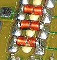
Passive components such as resistors , capacitors , quartz crystals or inductive components such as chokes are mainly produced in cuboidal designs. Two or more side surfaces of this design are designed to be solderable for electrical contacting. A perfect soldering of these "chips" can be recognized by a well-formed soldering meniscus .
At the beginning of SMD technology, transistors and integrated circuits were created from the (wired) dual-in-line housing ( DIL housing), a housing in which the solder connections of the component are led out on both side surfaces. The vertical solder connections of this housing were then simply bent either laterally outwards (English Gull-Wing ) or inwards (English J-Leads ) for the SMD soldering . With increasing integration density, especially with the processors with their many connections, further ways in connection technology were sought. This led to the development of the grid array connection technology. Here the solder connections are located as small metallized connection surfaces under the housing of the circuit. With the conventional ball grid array (BGA), there are already solder beads on the contact surfaces that are only melted on during the soldering process. In the land grid array (LGA), on the other hand, solder must be applied to the board to be assembled, which is why LGA components are rarely used for soldering. However, unlike BGAs, they can also be operated on a matching pin array. With an appropriately designed lock, LGA components can then simply be replaced, which z. B. is exploited in microprocessors.
- SMD connection types

SMD soldering surfaces on the side surfaces of the component such as B. with SMD ceramic multilayer capacitors (MLCC)
Gull-wing solder connections on the housing sides of an integrated circuit

J-lead solder connections on the housing sides of an integrated circuit (obsolete)

Solder beads under a microprocessor with BGA contact system

LGA contact surfaces arranged like a checkerboard under the housing of a microprocessor


SMD designs, SMD housings
There are two different generic terms in industry for the designs of SMD components. In the case of passive components (resistors, capacitors, inductors, crystals, etc.), the term design (English style ) is used for the different types of construction. The respective design can then also differ in terms of different dimensions and the type of connection form.
In the field of semiconductor technology and active components , on the other hand, the different designs are summarized by the generic term housing ( chip housing ). The active cell, the , which is installed in a housing, the justification for the different name. Each transistor or IC package has its own name derived from the first few letters of the English description. Deviations within the same housing designation, which result from the number and arrangement of the connections and the shape of the connections, are indicated by numbers appended to the name.
SMD designs of passive components, diodes and transistors
Passive components and possibly also diodes and transistors are manufactured, supplied and processed in the following designs:
- SMD designs

“Chip”, cuboid SMD chip design for capacitors and resistors with solder connection surfaces on the side surfaces of the housing

V-Chip , vertical cylindrical SMD design for aluminum electrolytic capacitors
Horizontal SMD design for resistors (Melf) and diodes (SOD)
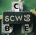
SMD transistor (BC817-40); Typical pin assignment: base / collector / emitter.


Chip, a cuboid design, is the typical design for MLCC and tantalum capacitors, inductors and non-linear and linear resistors (R chips). The term “chip” can easily be confused with the identical term from semiconductor technology, the “chip” (English “die”) of a semiconductor component. Cuboid special designs for z. B. Crystals or oscillators can also contain additional soldering surfaces on the housing, either for reverse polarity protection or for better and more vibration-resistant mechanical fastening.
The chip design of passive components differs mainly in the size, which is indicated with a code such as "1206". "12" stands for the length and "06" for the width of the component in the unit inch / 100. The dimensions have been standardized metrically, but only two digits are used when converting to the inch code, which leads to corresponding rounding errors. The length of a component marked with the code “1206” is 3.2 mm or 0.12598 inches, but only the “12” is used for the designation. If you calculate this back, you would only get 3.048 mm.
In the meantime, however, a metric coding of the size is becoming more and more popular.

| Case size, inch code |
Case size, metric code |
Housing length L in mm (± 0.2 mm) |
Housing width B in mm (± 0.2 mm) |
SMD-C chip (MLCC) |
SMD Ta chips 1) | SMD-R chip |
|---|---|---|---|---|---|---|
| 008004 | 0201 | 0.25 | 0.13 | X | ||
| 009005 | 03015 | 0.30 | 0.15 | X | - | X |
| 01005 | 0402 | 0.4 | 0.2 | X | - | X |
| 0201 | 0603 | 0.6 | 0.3 | X | - | X |
| 0402 | 1005 | 1.0 | 0.5 | X | - | X |
| 0603 | 1608 | 1.6 | 0.8 | X | - | X |
| 0805 | 2012 | 2.0 | 1.2 | X | R. | X |
| 1020 | 2550 | 2.5 | 5.0 | - | - | X |
| 1206 | 3216 | 3.2 | 1.6 | X | A. | X |
| 1210 | 3225 | 3.2 | 2.5 | X | - | X |
| 1218 | 3146 | 3.1 | 4.6 | - | - | X |
| 1225 | 3164 | 3.1 | 6.4 | - | - | X |
| 1411 | 3528 | 3.5 | 2.8 | - | B. | - |
| 1808 | 4520 | 4.5 | 2.0 | X | - | - |
| 1812 | 4532 | 4.5 | 3.2 | X | - | - |
| 2010 | 5025 | 5.0 | 2.5 | - | - | X |
| 2220 | 5750 | 5.7 | 5.0 | X | - | - |
| 2312 | 6032 | 6.0 | 3.2 | - | C. | - |
| 2512 | 6330 | 6.3 | 3.0 | - | - | X |
| 2917 | 7343 | 7.3 | 4.3 | - | D. | - |
| 2924 | 7361 | 7.3 | 6.1 | X | - | - |
| 1) Ta chips are identified with a letter code. They are manufactured in different heights | ||||||
Extended tables of the available chip sizes and their dimensions can also be found in the specialist articles for the components ceramic capacitors , tantalum electrolytic capacitors and resistors.
- V-Chip ( vertical chip ) is a cylindrical design with washers, mounted vertically. Aluminum electrolytic capacitors in particular are supplied and processed in this design. The sizes of this design are not standardized. V-chip aluminum electrolytic capacitors can be quite large; they are the exotic ones among the SMD components.
- MELF ( Metal Electrode Faces ) is the name for a cylindrical design of passive components that are mounted horizontally. It is the typical design for metal film resistors and non-linear resistors.
- SOD ( Small Outline Diode ) is the name of the cylindrical housing for the semiconductor component diode , which, like the MELF design, is also mounted horizontally. The SOD housing is also supplied in different sizes.
In addition, numerous passive components such as potentiometers , trimmers , transformers , transformers , crystals, oscillators have special SMD designs that are derived from the geometry and the connections of the components. The electromechanical components such as buttons, sockets, plugs and sockets, whose designs do not fit into common schemes, are also a special challenge.
SMD chip housings for semiconductors (transistors, integrated circuits)
Solder connections on two sides of the housing


SMD transistor housings with solder connections on two sides of the housing are identified with the following housing names:
- SOT ( small outline transistor ): design with three or four connections for transistors, the fourth connection is often designed as a heat sink , connection distance typically 1.27 mm
IC packages with solder terminals on two sides of the package are identified with the following package names:
- SOIC ( small-outline integrated circuit ): IC-SMD housing with the same row spacing as the through-hole version, the connection spacing is typically 1.27 mm
- SOP ( small outline package ): smaller version of the SOIC package , forms the basis for a whole series of modifications, some of which are manufacturer-specific, for example:
Solder connections on four sides of the housing

IC packages with solder terminals on the four sides of the package are identified with the following package names:
- PLCC ( plastic leaded chip carrier ): IC SMD housing with 20 to 84 "J-Lead" connections, housing with connection spacing of typically 1.27 mm.
-
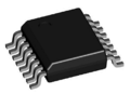
QFP ( quad flat package ): IC-SMD housing with 32 to 200 connections, forms the basis for a whole series of modifications, some of which are manufacturer-specific, for example:
- LQFP ( low-profile quad flat package ): IC-SMD housing with a height of 1.4 mm
- PQFP ( plastic quad flat package ): IC SMD package that has generally been replaced by the thinner TQFP package.
- CQFP ( ceramic quad flat package ): IC SMD package comparable to the PQFP package, but with a ceramic coating.
- MQFP ( metric quad flat package ): IC-SMD package comparable to the QFP package, but with metric spacing between the connections.
- TQFP ( thin quad flat package ): A thinner IC SMD package version of the PQFP package with a height of either 1.0 mm or 1.4 mm.
Solder connection surfaces under the housing, "leadframe" and "grid arrays"

- Quad flat no leads package (QFN), micro leadframe package (MLP), also micro lead frame , MLF: The names encompass a whole family of IC housings, the electrical connections of which are arranged like a frame around the side surfaces of the housing and act as metallized contact surfaces located under the housing. These cases sometimes have another metallized contact area under the housing, with the The connected to enable better heat dissipation. A variant MLPD (“D” stands for “dual”) is pin-compatible with the DIL-SOIC housing, with MLPD (dual) and MLPQ (quad) the connection configurations are differentiated, MLPM (micro) stands for a miniaturized version of the housing. The QFN-IC-SMD-housing is a special MLPQ-housing, the pin assignment and the connection distances correspond to the wired QFP-housing, but the metallized connection surfaces are attached as contact surfaces under the housing.
Highly integrated semiconductor components such as microprocessors have so many electrical connections that they can no longer be accommodated around the circumference of the housing. Therefore, these connections in the form of metallized connection surfaces are attached in a checkerboard or grid array under the housing. These semiconductor packages with solder connection surfaces in a checkerboard pattern under the package are identified by the following package names:
- LGA ( land grid array ): An LGA is a checkerboard or grid-like arrangement of electrical connection surfaces (English land ) on the underside of a housing for ICs with a large number of connections such as e.g. B. Microprocessors. When soldering these many contacts under the LGA housing, however, occasional soldering errors can occur that are very difficult to detect (X-ray). Since repairs are costly and faulty, LGA ICs are often placed on sockets. These sockets with the same pin assignment as the IC are soldered onto the board in the SMD process and can be tested for contact security quite easily. For the electrical connection, the processor is then pressed with its connection surfaces onto the upper contacts of the base with the aid of a clamp. The base has resilient contact pins so that reliable electrical contact can be made.

- BGA ( ball grid array ): Like the LGA housing, a BGA is a form of housing for integrated circuits in which the electrical connections are arranged in a checkerboard or grid-like arrangement on the underside. The connections are, however, in the form of small solder balls (engl. Balls ) is executed. During reflow soldering, these pearls are melted in a soldering oven and bond with the copper on the circuit board.
processing

Since the SMD components are assembled on a circuit board, this processing is called assembly , although the assembly also includes other work steps than just placing the components on the circuit board. These steps are:
- Applying solder paste (a mixture of tin balls and flux) or glue to the circuit board
- Equipping the components
- Soldering the circuit board or curing the adhesive
After each step, the quality of the product is optically checked before it is passed on to the next step. The production steps are usually carried out by machine, but machines are occasionally not used for individual pieces or in prototype construction or individual steps are carried out manually. The machines and processes required for processing are known as surface mounting technology. The area of an electronics factory that deals with the processing of SMDs is therefore referred to as the SMT area or SMT department.
Production lines for SMD assembly (principle)


The variants shown here can also be mixed with each other so that certain processes are controlled manually, others with automatic optical inspection. In some cases, a test step is completely omitted. For example, a final visual inspection can be omitted if the product is very simple because it is subjected to a functional test anyway. Individual tests are often already integrated into the production step. Modern paste printers, for example, have optics for checking the print and the cleanliness of the stencil.
Applying the solder paste or the adhesive

Solder paste or glue can be applied in several ways: Either it is applied using a screen printing process or it is added in small portions. The latter is mainly practiced manually in prototype and small series production. However, machines that meter the adhesive are also used to apply the adhesive. The adhesive is applied to the desired location through a thin tube or sprayed on without contact ( jetting ).
When applying the solder paste, the screen printing process has prevailed. Where component connections will later come to lie on the circuit board, this has copper surfaces - so-called pads - which are either gold-plated or tin-plated. The printing screen is positioned over the printed circuit board in such a way that the holes in the screen are centered over the pads. They are usually a few hundredths of a millimeter smaller to prevent the paste from being printed next to the pad.
The circuit board and screen are pressed against each other and a squeegee pushes the solder paste through the screen so that it gets through the holes onto the pads. The thickness of the screen determines the amount of tin (amount of solder paste) per area. In some cases, however, it is necessary that certain connections receive more tin - if this cannot be achieved with a larger pad area, additional solder paste must be added later.
The screens are now largely replaced by laser-cut metal templates. This means that smaller structures can be printed better. In order to achieve the required accuracy in printing, printers are used that allow the stencil to be precisely aligned with the circuit board. This can be done either by hand or automatically by a camera system which can recognize markings on the stencil and the circuit board and aligns the two with each other before printing.
Equipping the components
The smaller components are packed in cardboard or plastic belts. There are pockets in the straps in which the components are located. The top of the bag is closed by a film that is peeled off to remove the component, similar to a blister pack . The straps themselves are wound onto a roll. On at least one side of the belt there are transport holes at a distance of 4 mm through which the belt is moved by the pick and place machine. These rolls are fed to the pick and place machine with the help of feed modules .
ICs and other large components are often packaged in plastic sticks or in small pallets known as trays . While the trays can be inserted directly into the machine, feeders ( stickfeeder ) are also required for the rods . The vibration of the stick feeder causes the components to move forward after removal so that the placement head can remove the next component.
The components are removed with vacuum pipettes (English nozzle ) or grippers and then placed on the target position (X, Y coordinates) of the circuit board. This process is repeated for all components. When assembling the top of the board, gluing the components is usually not necessary, as the adhesive effect of the solder paste ensures the necessary adhesion of the component during the further transport of the board to the next station. After the circuit board has been fully populated, it is transported to the next processing station and a new circuit board can be accepted for assembly.
Curing the glue and soldering
In the case of glued-on SMD components, the adhesive is cured by heat. This is done in an oven that is also suitable for reflow soldering . In contrast to reflow soldering, the adhesive hardens at a lower temperature. After curing, the assemblies still have to be wave soldered . However, this happens after the THT assembly, provided that these THT components are also available.
If the assembly is intended for reflow soldering, it is brought to the required process temperature in a suitable reflow oven. The solder balls in the solder paste melt and ensure both a mechanical and an electrical connection between the component and the circuit board.
Typical mistakes
Some of the following errors only occur with reflow soldering, others only with wave soldering. In addition to the classic soldering defects, such as non-wetting and tin bridges, which also occur with push-through components, the following should be mentioned:
Tombstone effect

The grave stone effect ( English tombstoning ) occurs more often in components with two connections. The component stands out from the circuit board on one side, making it look like a small tombstone. It is now only soldered on at one point and the desired function is not given. If possible, you have to rework here manually. In addition to unfavorable soldering parameters, the too long storage of components is a cause when the connection surfaces are (differently) oxidized. SMD components that have already been soldered out tend to have a gravestone effect and are not suitable for reflow.
Popcorn effect

The popcorn effect ( English popcorning ) may arise if moisture-sensitive electronic components are stored for too long outside the protective packaging from moisture; they slowly absorb moisture from the ambient air. The storage of such moisture-sensitive components is regulated in IPC / JEDEC J-STD-020D (MSL classes, English Moisture Sensitive Level ). Due to the hygroscopic nature of the plastic housing of the components, water mainly accumulates in the housing casting compound and the structures to be protected (interconnects, substrate, etc.) (up to 0.5 percent by weight). In the reflow oven, the moisture evaporates due to the rapid rise in temperature, which leads to an expansion in volume. Consequences are u. a. Cracks in the housing and delamination of the substrate. The costly point of the popcorn effect is that it can only be diagnosed after production, if z. B. Devices with such components have already been sold in customer hands. Components that have been stored for too long or that have become damp can be dried inside again by so-called "baking" at approx. 110 ° C in 24 hours so that they are suitable for assembly or non-destructive soldering.
Blurring during the soldering process
A displacement in the X and / or Y direction of the SMD component is referred to as blurring . At the same time, additional twisting of the component can occur. Blurring can have different causes. Due to the surface tension of the liquid solder, the component changes its position. It is closely related to the tombstone effect.
Washing away of bonded components
If assemblies with glued SMD components are wave soldered, there is a risk that the liquid solder of the wave soldering system will loosen the adhesive connections between the circuit board and the component and thus the component will be washed off the circuit board and end up in the solder pot of the wave soldering system.
Non-wetting of bonded components
If assemblies with glued SMD components are wave soldered, there is also the risk that individual pins or individual components will not be soldered by the liquid solder of the wave soldering system. The shading caused by larger neighboring components can be seen as a possible cause for this. During wave soldering, these neighboring components can displace the solder flow in such a way that individual soldering points are not wetted by the solder and are therefore not soldered. After the soldering process, the affected components have open solder joints. Appropriate placement of the components when designing the circuit board avoids the problem. The design also defines the direction of flow through the soldering system.
See also
Web links
- Peter Zenker: SMD soldering made easy . (PDF)
- Detailed description for SMD soldering and desoldering at mikrocontroller.net
- Search for SMD code
Individual evidence
- ↑ spaceaholic.com, Artifact: Digital Computer Memory and Circuit Boards, LVDC, Saturn IB / V Guidance, Navigation and Control, spaceaholic.com
- ↑ Computerposter, computerposter.ch
- ^ "One chip" VHF radio IC, Philips data sheet TDA 7010, 1983
- ^ Valvo GmbH, Hamburg, At the pulse of time, 1974, anniversary publication for the 50th anniversary of Valvo GmbH
- ^ Günter Spur / Frank-Lothar Krause: The virtual product. Management of the CAD technology. Carl Hanser Verlag, Munich Vienna 1997, ISBN 3-446-19176-3
- ^ IBM 1966: Computer Aided Design Tools Developed for ICs, computerhistory.org
- ↑ Egon Fein, Grundig today, portrait of a global company, 1983, printing by Europrint GmbH
- ↑ Electronics 13/2002, WEKA-Fachzeitschriften-Verlag, special issue 50 years of electronics, electronics history, pages 84–88.
- ↑ a b c Valvo, SMD technology, components, assembly, processing, company publication p. 5, edited by HH Warnke, 1987 edition
- ^ Computer History Museum, 1965 - Package is the First to Accommodate System Design Considerations computerhistory.org
- ↑ Fairchild history, fairchildsemi.com
- ↑ Sprague, Dr. Preston Robinson Granted 103rd Patent Since Joining Company In 1929 mcla.edu (PDF)
- ↑ A. Fraioli, "Recent Advances in the solid-state Electrolytic Capacitor" IRE Tran. Comp. Parts, sanctions on Component Parts, June 1958.
- ↑ Preston Robinson, Sprague, US Patent 3066247, Aug. 25, 1954 - Nov. 27, 1962
- ^ Murata, Technical Report, Evolving Capacitors murata.com
- ↑ J. Ho, TR Jow, St. Boggs, Historical Introduction to Capacitor Technology, IEEE Electrical Insulation Magazine, Vol. 26, No. 1 (2010) ieeexplore.ieee.org
- ^ Larry E. Mosley, Intel Corporation, “Capacitor Impedance Needs For Future Microprocessors”, CARTS USA 2006, researchgate.net
- ^ C. Wiest, N. Blattau, J. Wright, R. Schatz, and C. Hillman, NIC, Robustness of Surface Mount Aluminum Electrolytic Capacitors When Subjected to Lead Free Reflow dfrsolutions.com (PDF) or niccomp.com (PDF )
- ^ J. Both, "The modern era of aluminum electrolytic capacitors," IEEE Electr. Insul. Mag., Vol. 31, no. 4, pp. 24-34, 2015. ieeexplore.ieee.org
- ↑ IEC-DIN-EN 60384-1, Fixed capacitors for use in electronic devices - Part 1: Basic specification beuth.de
- ↑ Miniaturization of the components can result in more rejects. Retrieved June 13, 2019 .
- ↑ Datasheet Rohm Ultra Compact Chip Resistors. Rohm Semiconductor, accessed June 13, 2019 .
- ↑ Will the first assembly machine for 03015 come in 2013? The smallest components in the world