
Chip package

The sheathing of a semiconductor chip (a die ) including the connection points (leads, pins or balls) is called a housing or package . There are numerous variations of such housings, which differ in their shape, the materials used, the number and arrangement of the pins and other properties.
This article covers the housing variants for integrated circuits , those for discrete components can be found in the list of semiconductor housings .
Standards
The chip housings are standardized by the JEDEC (formerly the Joint Electron Device Engineering Council , today the JEDEC Solid State Technology Association ), the semiconductor standardization committee of the EIA (Electronic Industries Alliance). In the case of electronic components, a basic distinction is made between wired, " Through Hole Technology " ( THT) and "surface-mounted" ( Surface Mounted Technologies - SMT) designs. " Surface Mounted Devices - SMD" refers to a component of the aforementioned group.
function
A housing is used to fasten the semiconductor chip on a circuit board and to connect the integrated circuit on the semiconductor chip with the components on the circuit board. The main reasons are, on the one hand, the protection of the die against damage. On the other hand, the different geometric distances between the electrical connections on a die and a printed circuit board must be bridged. The pads (connections of the IC die ) are bonded (connected) to an intermediate material using gold , copper or aluminum wire . This intermediate material is a stamped copper sheet ( leadframe ) or a small circuit board, which is called a substrate in this application . New technologies do without wires and use flip-chip technology . The connection to the circuit board is finally made via "legs" (pins) that are part of the leadframe, or via small solder balls (balls).
After the IC has been attached and wired to the intermediate material , it is protected against environmental influences by different materials ( plastic , ceramic , metal ). Ceramics and metals can hermetically seal the chip, while water molecules can diffuse through plastics. For cost reasons, plastic is almost exclusively used today by means of injection molding (technical term: molding). Depending on the type of semiconductor, openings for light (in the case of EPROMs for erasing, in the case of LEDs or laser diodes for the light exit) can also reveal the semiconductor. These openings are usually closed by means of transparent plastic or quartz glass so that the semiconductor is not directly exposed to the environment. Exceptions are sensors that have defined openings to measure environmental influences (e.g. pressure, light, etc.).
For better heat dissipation of the chip housing some have heat sink (heat sinks or heat spreaders ) installed (especially for power transistors).
In order to achieve a higher packing density, bare dies (“bare chips”) can also be mounted directly on the circuit board and encased there. If different dies are packed in one housing, one speaks of a multi-chip module .
The pins
The grid of the pins is called the pitch . Since the first ICs came from the Anglo-American language area, the dimensions were on an inch basis. The “basic dimension” was therefore the inch and the “mil” was usually used for small dimensions (1/1000 inch = 25.4 µm). In the course of internationalization, the metric dimensions are becoming more and more popular, so that typical pitches today at z. B. 0.5 mm.
The pins are usually placed on the side edges (e.g. DIL ) or the underside (e.g. PGA ) of the housing and have a wide variety of shapes. They are connected to the circuit board by soldering , the different shapes supporting the different types of soldering. Components in the THT housing are usually only placed on the component side of a circuit board. The assembled assembly is then soldered by wave soldering (the underside of the circuit board is drawn over a solder bath, at the end of which the bath creates a wave by damming, hence the name). With additional selective soldering , THT components can also be assembled and soldered on the second side of the circuit board. However, this is associated with an additional manufacturing step.
SMD components can be placed on the component side as well as on the solder side of the circuit board. Then they are soldered on both sides of the circuit board by reflow soldering or vapor phase soldering . Alternatively, SMD components can also be soldered by wave soldering. To do this, they must be on the solder side. The components must be wave solder resistant, i. H. the housing and the component itself must withstand the solder bath temperature. The pins must also not be short-circuited by the solder . Here the pin shapes and spacing are of crucial importance, so that only a few SMD designs, where the spacing is as large as possible, are suitable for this type of soldering. ICs with pins on all four sides of the housing must preferably be aligned diagonally to the direction of soldering during wave soldering so that as few tin bridges as possible are formed.
Some types of pins are also suitable for inserting the IC into a socket so that the IC no longer has to be soldered. (The socket still has to be soldered.)
With some components (especially powerful microprocessors) the number of pins is so high that the sides are no longer sufficient to accommodate the pins. That is why modern ICs often no longer have pins on the sides, but are attached to the circuit board using pins or solder balls on the underside of the housing ( ball grid array , BGA). With the solder balls, this only works with reflow soldering. Wave soldering is usually used for the pins on the bottom.
Different types
Since the JEDEC names are not very catchy, simpler abbreviations have established themselves in the industry, which can be described as quasi-standards. Acronyms are used as far as possible to describe the actual design.
Lead frame-based housing (engl. Lead frame based packages )
Designs for Through Hole Technology (THT)
- TO
- Transistor Single Outline: Different housings with mostly two or three connections for low power and power semiconductors (e.g. TO-220), there are also SMD versions
- PFM
- Plastic Flange Mount Package: Connections in a row below a mounting bracket, pitch 5.08 to 1.27 mm
- SIP
- Single in-line package , housing with one row of connections, usually with a 2.54 mm pitch
- ZIP
-
Zigzag Inline Package , connections on one side in zigzag, housing upright
- CZIP
- ZIP in ceramic housing
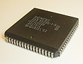
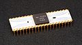
- DIL
- Dual in-line , housing with connections on two sides, mostly with a pitch of 2.54 mm (= 100 mil), the "archetype" of the chip housing
- DIP
-
Dual in-line package , like DIL
- PDIP
- Plastic Dual In-Line Package, like DIP in a plastic housing
- SDIP
- Shrink Dual In-Line Package, like DIP with smaller dimensions, pitch 2.54 to 1.27 mm
- CDIP
- Glass Sealed Ceramic Dual In-Line Package, like DIP in a ceramic housing
- CDIP-SB
- Side-Braze Ceramic Dual In-Line Package, like DIP in a ceramic housing
Designs for Surface Mounted Device (SMD)
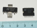
- TO or DPAK
- Transistor Single Outline: also exists as a THT version and is used for power transistors (e.g. DPAK / TO252, D2PAK / TO263)
- SOD
- Small Outline Diode: For diodes
- SOD80
- 3.7mm x 1.6mm
- SOD123
- 2.675mm x 1.6mm x 1.15mm
- SOD223
- 6.5mm × 3.5mm × 1.65mm
- SOD323
- 1.7 mm × 1.25 mm × 0.95 mm
- SOD523
- 1.2mm × 0.8mm × 0.6mm
- SOT
- Small Outline Transistor: For transistors
- SOT23
- 3 mm x 1.75 mm x 1.3 mm
- SOT223
- 6.7 mm × 3.7 mm × 1.8 mm with 4 connections, one of which is widened as a heat sink
- SOT323
- 2.2 mm x 1.35 mm x 1.1 mm
- SOT143
- 3 mm × 1.4 mm × 1.1 mm
- DFP
- Dual Flat Pack, pins on both long sides, pitch 0.65 mm
- TFP
- Triple Flat Pack, pins on three sides, 0.8 mm pitch
- QFP
-
Quad Flat Package , pins on four sides, grid 1.27 to 0.4 mm, various derivatives were derived from this basic type, each of which prefixes a different letter:
- LQFP
- Low Profile Quad Flat Pack, like QFP, thin case
- TQFP
- Thin Quad Flat Pack, like QFP, thin case
- VQFP
- Very Thin Quad Flat Pack, like QFP, very thin housing, pitch 0.8 to 0.4 mm
- HQFP
- Thermally Enhanced Quad Flat Pack, like QFP, thermally reinforced
- MQFP
- Metric Quad Flat Pack, like QFP, pins are metric spaced
- QFN
-
- Quad Flat No Leads Package , also known as MLF Micro Lead Frame, or as MFP for Micro lead Frame Package: The names encompass a whole family of IC packages. The pins do not protrude laterally beyond the dimensions of the plastic coating, but are only accessible from the underside, so they take up less space;
- VQFN
- Very Thin Quad Flat pack No-leads, like QFN, very thin housing
- SOP
-
SOIC - Small-Outline Package , mostly in a 1.27 mm grid
- SSOP
- Shrink Small Outline Package, smaller grid than SOP, mostly 0.65 mm, also flatter
- TSSOP
- Thin Shrink Small Outline Package , flatter than SSOP
- TSOP
- Thin Small Outline Package , like SOP, but mostly with a grid of 0.635 or 0.65 mm
- HTSSOP
- Heat-Sink Thin Small-Outline Package, like TSOP, with pad for heat dissipation or metal back
- TVSOP
- Thin Very Small-Outline Package, like TSOP, thinner housing
- QSOP
- Quarter-Size Small-Outline package, also smaller than SOP, i. d. Usually in a grid of 0.635 mm
- VSOP
- Very Small-Outline Package, like SOP, smaller grid
- HSOP
- Thermally Enhanced Small-Outline Package, like SOP, thermally reinforced
- SOY
-
J-Leaded Small-Outline Package , the pins are bent under the housing so that they are suitable for sockets
- JLCC
- J-Leaded Ceramic or Metal Chip Carrier, such as SOJ
- PLCC
- Plastic Leaded Chip Carriers , such as SOJ
- LPCC
- Leadless Plastic Chip Carrier, such as PLCC
- LCCC
- Leadless Ceramic Chip Carrier, like PLCC in a ceramic package
Substrate-based housing
Designs for Surface Mounted Device (SMD)
- LGA
-
- Land grid array , package with contact areas on the bottom
- TVFLGA
- Thin Very-Fine Land Grid Array, like LGA, with a smaller grid
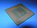
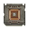
- PGA
-
Pin grid array , package with pins on the underside, if the pins are arranged offset, this is called a staggered pin grid array (SPGA)
- PPGA
- Plastic Pin Grid Array , like PGA in a plastic housing
- CPGA
- Ceramic pin grid array , like PGA in a ceramic housing
- OPGA
- Organic pin grid array , like PGA in an "organic" plastic housing
- FCPGA
- Flip-Chip Pin Grid Array
- BGA
-
Ball Grid Array , package with small solder balls on the bottom
- FBGA
- Fine pitch BGA , BGA package with reduced solder point spacing
- FCBGA
- Flip Chip Ball Grid Array
- CBGA
- Ceramic Ball Grid Array, like BGA in a ceramic housing
- MAPBGA
- Mold Array Process BGA
- CSP
- Chip scale package , particularly small form of the BGA
- HSBGA
- Heat Slug Ball Grid Array
- CCGA
- Ceramic Column Grid Array , higher reliability thanks to cylindrical connections instead of spheres
Special shapes
- TCP
- Tape Carrier Package : The one with bumps on copper-clad foil
gallery
- different chip housings

SIL9 TDA4601 with cooling plate

DIL28 UV ST6E15 1989

Piggyback40 Toshiba TLCS90 Family 1988

DIL18 Microchip PIC16F84

DIL28 Atmel AT90S2333

ZIP19 (20) Toshiba DRAM 514256 1990

ZIP28 Toshiba VideoRAM 524256 1992

TO-5 metal housing, OP : 1979
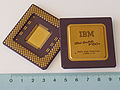
PGA 6x86 IBM
PGA AMD

PGA 486DX2 AMD, opened with a view to the die

CPGA and PPGA of the Pentium family
Power-DIP, Power-SO

BGA16 (NEC 78K0S) and SOT23-6 (Microchip PIC)

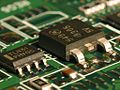
Various SMD components

SO20 UV ST6E20, 1992

CRQFP80 UV erasable ST62E40, 1993

TQFP216 AMD Am286LX / ZX (SoC)

bumped TQFP132 on the Intel i386SL

U80701 in CQFP housing with carrier

PLCC20 (28) IBM Memory 1991
PLCC68 80286 Siemens, 1989

PLCC84 UV Cypress FPGA, 1996

CLCC68: Intel R80C188XL. Seen from above left and right from below

LGA775

CQFN44 Harris 82C55, 1993

TQFP leadframe

DIP16 lead frame

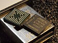
EPROM-Die by 'Bulleye'

80486-Die in the opened case

SOT23 or SC70 still unsoldered in solder paste
Various SMD components (SO8 and DPAK)

PCB, memory module or SIMM (PLCC18)

BGA: Embedded Intel Pentium MMX
FBGA: Two CPLDs on one USB connector

Plastic DIL64: Thomson TS68000 (= Motorola MC68000)
Ceramic DIL40: AMI S6800 (= Motorola MC6800)

Circuit board, Slot-A Athlon AMD
Intel Pentium as TCP version

SOT23-6 package


_Toshiba_DRAM_514256.jpg)


_Memory.jpg)


Web links
- Housing shapes on microcontroller wiki
- Housing from TI: According to various selection criteria (including JEDEC)
- National Semiconductor package (overview with pictures) ( Memento of October 28, 2012 in the Internet Archive )