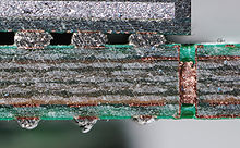
Via
Through-hole plating (ugs. Durchsteiger , English vertical interconnect access , short: VIA) is a vertical electrical connection between the conductor track levels of a printed circuit board . The connection is usually realized through an internally metallized hole in the substrate of the circuit board. Rivets and pins are also rarely used.
Vias are also found in integrated circuits (IC). Vertical electrical connections between two metallization levels are referred to here as vias , while contact holes ( contacts ) are used for the connections between the lowest (first) metallization level and the underlying silicon (diffusion layer or poly level). Another form of IC vias are silicon vias that enable vertical electrical connections between stacked microchips in 3D integrated ICs.
Manufacturing
Vias are produced by seeding the hole in the carrier material (covered with a catalyst ), then catalytically metallizing it and then, if necessary, electrolytically reinforcing it (building a thicker metal layer). This technology differs from the production of the conductor tracks (these can be manufactured with a mask etching process), corresponding circuit boards are called through-hole circuit boards (DKL). Printed circuit boards without vias are accordingly referred to as NDKL.
Individual soldering eyes can also be retrofitted purely mechanically using through-hole rivets, see illustration.
IC vias are produced step by step by etching metal layers or depositing metal in structured dielectric layers , cf. u. a. Damascene and dual damascene process .
commitment
The plated through hole can simultaneously serve as a soldering eye for wired components ( through hole ) or it can only be attached for the purpose of making electrical contact.
Vias can also or exclusively serve to improve vertical heat conduction ( thermal vias ).
To reduce the line inductance or to increase the current-carrying capacity, several vias are often introduced in parallel for a connection.
Executions
Depending on the intended use, the diameter and possibly the shape are different. Smaller vias are drilled during the manufacture of printed circuit boards. In addition, there is the possibility that larger plated-through holes can be milled and thus other geometries (for example elongated holes ) can be produced.
With the help of plated-through holes, it is possible to change the conductor levels in two- or multi-layer circuit boards. This is the prerequisite for disentangling complex circuits .
If the hole of the via has a very small diameter, it is also called a micro via . Micro vias are often drilled with a laser .
If the plated-through hole does not extend through the entire board, but only to one of the middle layers, it is called blind via . If there are vias "buried" only between the middle layers, they are called buried via .
Assembly
SMD components
Wired components are increasingly being replaced by non-wired surface mounted devices , which is why today's printed circuit boards have a larger number of vias that do not accept any component. There should be no vias in the area of SMD soldering points, since liquid solder can flow into the via during soldering and thus lead to a lean soldering point. However, if through-plating in the pad area of SMD components cannot be avoided, a sufficient amount of solder must be provided by applying thicker solder paste. There is also the possibility of covering or sealing the vias with adequate methods.
THT components
When (wired) components are soldered in vias, the vias are filled with solder. This improves the connection between the component and the printed circuit board, but this tin must be removed again when the components are desoldered , which makes repairs to such assemblies difficult.
PCB robustness
Through-plated circuit boards provide a better hold and more reliable connection of wired components. They are therefore common even with simple, high quality assemblies. In addition to the adhesive connection of the individual layers of the circuit board, the metallized vias ensure better cohesion of the circuit board.
Web links
Individual evidence
- ^ KH Cordes, A. Waag, N. Heuck: Integrated circuits . Pearson, 2011, ISBN 978-3-86894-011-4 , chap. 4.6.3 Contacts and vias .
- ↑ J. Knechtel, O. Sinanoglu, IM Elfadel, J. Lienig, CCN Sze: Large-Scale 3D Chips: Challenges and Solutions for Design Automation, Testing, and Trustworthy Integration . In: IPSJ Transactions on System LSI Design Methodology . 10, 2017, pp. 45-62. doi : 10.2197 / ipsjtsldm.10.45 .


