Chemical vapor deposition
The term chemical vapor deposition ( English chemical vapor deposition , CVD), rarely chemical vapor deposition , are a group of coating methods , which, inter alia, in the production of microelectronic components and optical fibers are used.

history
The term chemical vapor deposition was coined in 1960 by John M. Blocher , Jr. This term was used to distinguish chemical vapor deposition from physical coating processes, which John Blocher summarized under the term PVD ( physical vapor deposition ).
However, the history of the process begins much earlier. As early as 1852, the German chemist Robert Wilhelm Bunsen reported on the separation of Fe 2 O 3 from gaseous iron chloride (FeCl 3 ) and water vapor. Depending on the definition of the term, significantly older reports on CVD processes can also be found.
Procedural principle
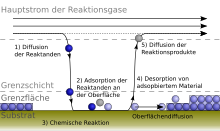
Due to a chemical reaction from the gas phase, a solid component is deposited on the heated surface of a substrate .
The prerequisite for this is that there are volatile compounds of the layer components that deposit the solid layer at a certain reaction temperature.
The chemical vapor deposition process is characterized by at least one reaction on the surface of the workpiece to be coated. At least one gaseous starting compound ( starting material ) and at least two reaction products - at least one of which in the solid phase - must be involved in this reaction .
Chemical vapor deposition processes are mostly operated at reduced pressure (typically 1–1000 Pa) in order to promote those reactions on the surface compared to competing gas phase reactions and thus avoid the formation of solid particles.
A special feature of the process is the conformal layer deposition. In contrast to physical processes, chemical vapor deposition also enables complex three-dimensional surfaces to be coated. So z. B. finest depressions in wafers or hollow bodies are coated evenly on their inside.
Precise deposition can also be achieved with the help of focused electron or ion beams . The charged electrons or ions cause the substances dissolved in the gas to be deposited in the irradiated areas. Such electron beams can be generated, for example, with a synchrotron or a scanning electron microscope . The ion beams can be generated with an FIB device . These also enable selective gas-assisted ion beam etching.
Examples
- Synthetic crystalline diamond layers are deposited from a gas phase which generally consists of around 99% by volume of hydrogen and only around 1% by volume of a carbon source (methane, acetylene). The gases are activated either thermally, with the help of a plasma or a laser. The excess of hydrogen suppresses, among other things, the simultaneous formation of sp²-hybridized carbon species (graphite, amorphous carbon).
- A silicon nitride layer is produced from ammonia and dichlorosilane .
- Silane and oxygen or TEOS ( tetraethylorthosilicate ) and oxygen are used for silicon dioxide layers .
- Tungsten hexafluoride is used to produce metal / silicon hybrids (silicides) .
- Titanium nitride layers for hardening tools (drills, cutting tools) are produced from TDMAT and nitrogen.
- Tin oxide layers are deposited from tin chloride or tin organic compounds and oxygen or water vapor on flat glass and on container glass.
- Silicon carbide layers are deposited on hot surfaces (above approx. 800 ° C) from a mixture of hydrogen and methyl trichlorosilane (CH 3 SiCl 3 ).
- Fields of carbon nanotubes can be synthesized on a substrate .
application
Coatings are used in the electronics industry to e.g. B. Si 3 N 4 , SiO 2 , poly-Si, crystalline Si (Epi-Si) and SiON x to be deposited on wafer surfaces.
Before the deposition, the wafer is cleaned in a dry etch process , in which either sulfur hexafluoride or a mixture of tetrafluoromethane and high-purity oxygen are used. Nitrogen and hydrogen serve as carrier gases. The CVD reaction chambers are cleaned with nitrogen trifluoride .
For the structuring of silicon by etching processes, an epi-Si layer doped with boron can be deposited as an etch stop layer by means of gas phase epitaxy .
Outside of the electronics industry, the refinement of glass and the manufacture of fiber optic cables for optical communications technology are one of the largest areas of application for chemical vapor deposition. Every year around 10 million m² of architectural glass are coated with thermal protection layers made of fluorine-doped tin oxide. Another important application of tin oxide layers is to protect container glass. The coating on the outer surfaces protects the glass against mechanical shock loads, for example in bottling plants. Further applications are optical layers on glass, on plastic and gas-tight barrier layers.
Boron-doped CVD diamond electrodes are u. a. used in industrial water treatment for wastewater oxidation and disinfection of process water.
Procedural limits
Not every desirable layer has a gaseous compound from which it could be made.
Another limitation of the process is the high temperature load on the substrate. The heat load can, among other things, cause distortion on workpieces or lie above the softening temperature of the material to be coated, so that the process cannot be used. In addition, diffusion processes occur at high temperatures, which means that doping profiles are smeared or metals diffuse in after coating processes. However, there are also variants in which the thermal load is lower and thus the negative effects are reduced.
variants
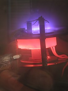
The temperature load on the substrate can be reduced by means of the plasma-enhanced chemical vapor deposition ( plasma enhanced CVD , PECVD ). A plasma is ignited above the wafer . This can be done either inductively ( inductively-coupled PECVD , ICPECVD) or capacitively ( capacitance-coupled PECVD ). This CVD process takes place at temperatures between 200 and 500 ° C. Since the thermal energy for pyrolysis is insufficient at these temperatures , the gas is excited and decomposed by a plasma. Furthermore, the deposition rate is increased by the plasma excitation. However, there is the disadvantage here that the crystal structure of the wafer is damaged by the radiation from the plasma . In addition to these direct plasma processes, there is also RPECVD ( remote plasma enhanced CVD ), in which the plasma is spatially separated from the substrate. This reduces the stress on the substrate from ion bombardment and radiation.
The HFCVD process (ger .: hot filament CVD , dt. "Hot wire-activated chemical vapor deposition"), and hot-wire CVD or catalytic CVD called the film deposition possible by the recipient stretched filaments (wires), which are usually made of tungsten , tantalum or rhenium . An applied voltage causes the filaments to glow, with wire temperatures of up to 2600 ° C being reached. The gases used are split into radicals by these high temperatures on the filaments and the species thus formed ensure the layer structure (e.g. production of polycrystalline diamond layers).
Low pressure CVD ( low pressure chemical vapor deposition , LPCVD) is the method frequently used in semiconductor technology for the deposition of silicon oxide, silicon nitride and poly-silicon, as well as metals. The process takes place in tube furnaces, nowadays mostly in vertical furnaces.
APCVD (ger .: atmospheric pressure chemical vapor deposition , Eng. »Chemical vapor deposition at atmospheric pressure ") is operated in contrast to most CVD processes, not at a reduced, but at normal pressure.
With metal-organic chemical vapor deposition (engl .: metal organic chemical vapor deposition , MOCVD, also: OMCVD) the chemical deposition from organometallic starting compounds is referred to. A subgroup of the MOCVD is gas phase epitaxy ( metal organic vapor phase epitaxy , MOVPE ), in which very high quality crystalline layers are produced. In the field of compound semiconductor production such. B. III-V and II-VI semiconductors , these terms are used for identical processes, depending on the language area.
To be able to coat a specialty that uses the special advantage of the CVD method, porous body evenly, the chemical vapor infiltration (ger .: chemical vapor infiltration , CVI). This method is used e.g. B. used for coating fiber bundles.
| CVD variant | typical working temperature | typical work pressure | Activation energy | Uses |
|---|---|---|---|---|
| APCVD | 400-1300 ° C | 1 bar | thermally activated | Deposition of poly-Si for conductor tracks, gate oxide, epitaxy of Si wafers |
| LPCVD | 500-1000 ° C | 0.01-10 mbar | thermally activated process | Conductor tracks, silicon dioxide , silicon nitride , poly-silicon |
| HFCVD | 150-1100 ° C | 0.01-200 mbar | thermally activated process | Carbon-based deposition ( diamond , amorphous carbon , carbon nanotubes ), silicon- based layers ( amorphous / crystalline Si, Si 3 N 4 , ...) |
| PECVD | 200-500 ° C | 1 mbar | plasma + thermal | Separate SiO 2 ⇒ passivation Si 3 N 4 ⇒ passivation |
literature
An excellent overview of chemical vapor deposition can be found in the classic "Vapor Deposition" by Powell et al. which, despite its age, is still very current in the basics.
- CF Powell , JH Oxley, JM Blocher Jr., J. Klerer: Vapor Deposition . In: Journal of The Electrochemical Society . tape 113 , no. 10 , 1966, pp. 266C-269C , doi : 10.1149 / 1.2423765 .
- KL Choy: Chemical vapor deposition of coatings . In: Progress in Materials Science . tape 48 , no. 2 , 2003, p. 57–170 , doi : 10.1016 / S0079-6425 (01) 00009-3 (very detailed recent review article in which, in addition to the individual processes, the advantages and disadvantages of the individual reactor types are described).
- Hugh O. Pierson: Handbook of chemical vapor deposition (CVD): principles, technology, and applications . William Andrew, 1999, ISBN 978-0-8155-1432-9 .
- M. Allendorf: From bunsen to VLSI: 150 years of growth in chemical vapor deposition technology . In: The Electrochemical Society interface . tape 7 , no. 1 , 1998, p. 36–39 ( PDF file; 131 kB ).
- CA Volkert, AM Minor, others: Focused ion beam microscopy and micromachining . In: MRS bulletin . tape 32 , no. 5 , 2007, p. 389–395 ( PDF file; 2.42 MB ( memento of September 29, 2007 in the Internet Archive )).
Individual evidence
- ↑ Mark Allendorf: From bunsen to VLSI: 150 years of growth in chemical vapor deposition technology . In: The Electrochemical Society interface . tape 7 , no. 1 , 1998, p. 36–39 ( PDF file; 131 kB ).
- ^ Mark Allendorf: On-line Deposition of Oxides on Flat Glass . In: The Electrochemical Society Interface . tape 10 , no. 2 , 2001 ( PDF ).
- ↑ reflectors .
- ↑ Plastic applications .
- ↑ barrier layers
- ↑ Artificial diamond layers .
- ↑ Crystec Technology Trading GmbH, PECVD processes in the semiconductor industry . Retrieved December 17, 2010.
- ↑ Crystec Technology Trading GmbH, LPCVD processes in the semiconductor industry . Retrieved December 17, 2010.
Web links
- Daniel M. Dobkin: Fundamentals of Chemical Vapor Deposition . (Online tutorial on the basics of chemical vapor deposition, English)
- Markus Winterer: Chemical Vapor Deposition and Chemical Vapor Synthesis . University of Duisburg Essen (lecture slides, PDF file; 6 MB)
- Introduction: Focused Ion Beam Systems . Fibics (principle of the CVD technique with the help of FIB, English).
