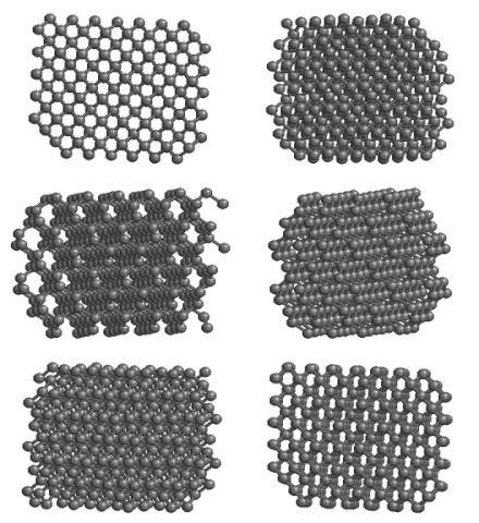
Grid guide effect
The grid guidance or the grid guidance effect ( English channeling ) is a physical phenomenon that occurs in ion beam physics . It describes the almost undisturbed penetration of an ion into a single crystal due to linear areas without lattice atoms in certain crystal lattices .
description

If single crystals are irradiated with bundled ions at an angle close to a crystal axis, they penetrate deep into the crystal. In typical backscattering experiments ( Rutherford backscattering ), a lower backscatter rate is measured because the collision with lattice atoms becomes less likely along the crystal axis. If the atoms were lined up in a perfect row, the ions would only see a single plane ; it is as if the particles penetrate along the lattice through channels, even held by the repulsive effect of the lattice atoms in the channel (since both are positively charged), which explains the English and German names.
If the particles are detected two-dimensionally, typical backscattering patterns are obtained, which depend on the crystal structure , the special crystal axis and the lattice location of the backscattering atoms. This also speeds up the measurement compared to one-dimensional detectors.
Even negative and neutral particles show the grid guide effect. The experiment can also be carried out with radioactive ions. In this case it is no longer the ions, but the particles emitted by them that are detected; this is called emission channeling (Engl. emission channeling ).
history
This effect was foreseen even before the first experiments with X-ray radiation showed diffraction effects on single crystals. Such a hypothesis was published in 1912 ( Johannes Stark ). More than 50 years later came the first experimental evidence (Piercy et al., 1963) and the first computer simulations (Robinson and Oen, 1963). In the meantime, the studies on this effect have experienced a very good, if not completely mature, theoretical and experimental development.
Applications
A direct application of this technique is the determination of the crystal structure and the distribution and position of defects or impurities in a sample (e.g. thin layers). A more interesting application is, for example, the determination of the lattice position when a radioactive isotope of the normally stable elements is used to dop a semiconductor in the production of microelectronic circuits . Since the radiation emanates directly from the doping points after doping, the distribution and position of the doping points and thus the semiconductor properties can be determined much more precisely compared to methods that work with external radiation sources (e.g. X-ray structure analyzes). The lattice guidance effect not only affects the doping, but also contributes to the directional dependence of the radiation produced (with α and β radiation). Other applications are in surface physics (surface relaxation, surface contamination, structural analysis at the interface between two different layers, etc.).
Significance in the semiconductor industry
The grid guidance is an undesirable effect in the manufacture of semiconductor components. Here, silicon wafers are specifically doped with foreign atoms in order to obtain the desired electrical properties. One possible method for doping (besides diffusion ) is ion implantation , in which the wafer is bombarded with ions. This is where the effect occurs and changes the otherwise very well simulated penetration depth of the ions.
The grid guidance can be counteracted in two ways: on the one hand, by tilting the wafer slightly in relation to the direction of implantation (approx. 7 °). Alternatively or in addition, a thin layer of silicon dioxide is produced on the wafer before the implantation (with a coating process or by thermal oxidation ). The ions are scattered on this amorphous layer by elastic and inelastic collisions and so no longer penetrate preferentially along the crystal planes.
literature
- James W. Mayer, E. Rimini: Ion Beam Handbook for Materials Analysis . Academic Press Inc, New York 1977, ISBN 0-12-480860-3 .
- Leonard C. Feldman: Materials Analysis by Ion Channeling: Submicron Crystallography . Academic Press Inc, New York 1982, ISBN 0-12-252680-5 .
- H. Erramli, G. Blondiaux: Ion chanelling . In: Applied Radiation and Isotopes . tape 46 , 6-7 (June / July), 1995, pp. 413-418 , doi : 10.1016 / 0969-8043 (95) 00032-1 .
Individual evidence
- ↑ Johannes Stark: Dispersion and absorption of β-rays and X-rays . In: Physikalische Zeitschrift . tape 13 , 1912, pp. 973-977 .
- ↑ GR Piercy, F. Brown, JA Davies, M. McCargo: Experimental evidence for the increase of heavy ion ranges by channeling in crystalline structure . In: Physical Review Letters . tape 10 , May 1, 1963, pp. 399-400 , doi : 10.1103 / PhysRevLett.10.399 .
- ↑ Mark T. Robinson, S. Ordean Oen: Computer Studies of the Slowing Down of Energetic Atoms in Crystals . In: Physical Review . tape 132 , no. 6 , December 15, 1963, pp. 2385 , doi : 10.1103 / PhysRev.132.2385 .
- ↑ Mark T. Robinson, S. Ordean Oen: The channeling of Energetic Atoms in Crystal Lattices . In: Applied Physics Letters . tape 2 , no. 2 , January 15, 1963, p. 30-32 , doi : 10.1063 / 1.1753757 .
- ^ Leonard C. Feldman, James W. Mayer, Steward TA Picraux: Materials Analysis by Ion Channeling: Submicron Crystallography . Academic Press, 1982, ISBN 0-323-13981-7 , pp. xii and following ( limited preview in Google Book Search).
- ↑ James Mayer: Ion Implantation in Semiconductors: Silicon and Germanium . Elsevier Science, 1970, ISBN 0-323-15721-1 , pp. 130–135 ( limited preview in Google Book search).