Glue logic

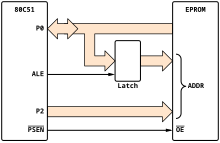
The English term glue logic (German: “adhesive logic ” in the sense of connection logic ) refers to a relatively simple logic circuit that was designed to connect two initially incompatible hardware components. The glue logic itself has no further use other than connecting the components. A typical example is a circuit ( memory controller ) for interconnecting a microprocessor with DRAM modules; DRAM has a different bus structure than conventional microprocessors and is usually much slower, so the two components cannot be connected directly. Further examples are address decoding, i.e. the generation of chip select signals from the addresses on the address bus, and the (de) multiplexing of bus signals (see figure).
Today glue logic is almost exclusively implemented using programmable logic modules (mostly FPGAs and CPLDs ); In the past, collections of 74xx chips or other simple logic chips were often used as glue logic .