Anodic bonding
Anodic bonding is a connection process that is used particularly in the manufacture of sensors and micromechanical components in semiconductor and microsystem technology .
Procedure
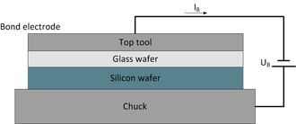
A silicon wafer with a polished surface and a very flat wafer made of a glass that contains alkali ions (similar to window glass) are placed on a heating plate. The heating plate is heated to approx. 300 to 400 ° C. The silicon wafer lies directly on the heating plate and above the glass wafer. A point electrode is now lightly pressed onto one point of the glass wafer. The heating plate is the counter electrode. The silicon wafer is sufficiently intrinsically conductive at these temperatures . The heating causes the ions in the glass, e.g. B. potassium and sodium , can move more freely. If an external voltage is applied in such a way that the glass wafer is negatively charged and the heating plate positively charged, the ions in the glass slowly migrate to the point electrode. This charge transport reduces the amount of ions on the surface of the glass towards the silicon wafer, i.e. this area is negatively charged. A space charge zone is created .
At the same time, the silicon wafer is positively charged by the external voltage. This is how both surfaces attract each other. Due to the very smooth and even surfaces of silicon and glass, there is only a very small gap between the two. The attraction of opposing electrodes increases when the distance is reduced ( Coulomb's law ). So both surfaces are drawn closer and closer together. Finally, a point has been reached where the distance is so small that the surface atoms of the glass can chemically react with those of the silicon. Chemical bonds are formed between the silicon of the silicon wafer and the oxygen from the silicon oxide of the glass, although the actual reaction temperature has not yet been reached.
This process can be followed optically: starting from the point electrode, a dark, circular front spreads over the entire surface. The greater the distance from the point electrode, the slower this front moves. Small disturbances of the surface or particles lead to gas inclusions . After switching off the voltage and cooling, the two wafers can no longer be separated from one another. If you try anyway, the break is mostly in the glass, but not at the interface between glass and silicon .
Applications
The method is used in the manufacture of pressure sensors that are used e.g. B. can also be used in automotive electronics.
See also
Individual evidence
- ↑ Anodic bonding. Surface connection of a silicon wafer with a glass substrate ( memento of the original from November 8, 2016 in the Internet Archive ) Info: The archive link was automatically inserted and not yet checked. Please check the original and archive link according to the instructions and then remove this notice. . Esslingen University of Applied Sciences, accessed on November 8, 2016.
