In order to be able to calculate the behavior of a bipolar transistor or field effect transistor in complex circuits, one needs a simplified, abstract model . Different levels of abstraction are used here. Usually simple models are used for dimensioning and more complex models or their equivalent circuit diagram for circuit simulation .
Theoretically, an exact calculation of the physical behavior would also be possible, for example using a Monte Carlo simulation , but even in relatively simple electrical networks, the computational effort of such a simulation exceeds the performance of today's computers. The models therefore serve to simplify and adequately simulate the real processes in order to drastically reduce the computing effort.
A further simplification can be achieved by using different models for static and dynamic operation. The former are used for DC dimensioning, and thus primarily for calculating the correct operating point setting , as well as for low-frequency logic circuits (e.g. TTL ). Models for dynamic operation are used for alternating current dimensioning and thus for calculating circuits for signal transmission and signal processing .
This article deals exclusively with the modeling of the bipolar transistor, for information on the construction and use of bipolar transistors please refer to the main article .
Formula symbol
The symbols used here are listed below. For further symbols see also the mathematical description .
| character |
description
|
 |
Ideal base current of the emitter diode
|
 |
Ideal base current of the collector diode
|
 |
Base leakage current of the emitter diode
|
 |
Base leakage current of the collector diode
|
 |
Collector-emitter transport current
|
 |
Current of the substrate diode
|
|
 |
Base resistance
|
 |
Collector path resistance
|
 |
Emitter resistance
|
|
 |
Junction capacitance of the emitter diode
|
 |
Internal junction capacitance of the collector diode
|
 |
External junction capacitance of the collector diode
|
 |
Junction capacitance of the substrate diode
|
 |
Diffusion capacitance of the emitter diode
|
 |
Diffusion capacity of the collector diode
|
Formula symbols for the static and dynamic behavior
Formula symbol for the static behavior
| character |
description
|
 |
Reverse saturation current
|
 |
Saturation reverse current of the substrate diode
|
 |
Ideal current amplification in normal operation
|
 |
Ideal current amplification in inverse operation
|
|
 |
Leakage saturation reverse current of the emitter diode
|
 |
Leakage saturation reverse current of the collector diode
|
 |
Emission coefficient of the emitter diode
|
 |
Emission coefficient of the collector diode
|
|
 |
Knee current for strong injection in normal operation
|
 |
Knee current for strong injection in inverse operation
|
|
 |
Temperature voltage (approx. 26 mV at room temperature)
|
|
 |
Early voltage in normal operation
|
 |
Early voltage in inverse operation
|
|
 |
External rail resistance
|
 |
Internal rail resistance 1)
|
1) is calculated in PSpice from the equation .
|
|
Formula symbol for dynamic behavior
| character |
description
|
 |
Zero capacitance of the emitter diode
|
 |
Zero capacitance of the collector diode
|
 |
Zero capacitance of the substrate diode
|
 |
Diffusion voltage of the emitter diode
|
 |
Diffusion voltage of the collector diode
|
 |
Diffusion voltage of the substrate diode
|
 |
Capacitance coefficient of the emitter diode
|
 |
Capacity coefficient of the collector diode
|
 |
Capacity coefficient of the substrate diode
|
|
 |
Distribution coefficient of the capacitance in the collector diode
|
 |
Coefficient for the course of capacity
|
|
 |
Ideal transit time in normal operation
|
 |
Ideal transit time in reverse operation
|
 |
Transit time coefficient in normal operation
|
 |
Transit time coefficient in inverse operation
|
 |
Transit time voltage in normal operation
|
 |
Transit time voltage in inverse operation
|
 |
Transit time stream in normal operation
|
 |
Transit time flow in inverse operation
|
|
More formula symbols
Formula symbol for the thermal behavior
| character |
description
|
 |
Temperature coefficient of the reverse currents
|
 |
Temperature coefficient of the current gain
|
English name
Since data sheets are mostly written in English, one must also be able to translate the symbols used. These are essentially:
| German
|
English
|
| designation |
character |
designation |
character
|
| tension |
U |
voltage |
V
|
| Normal operation |
N |
forward region |
F.
|
| Inverse operation |
I. |
reverse region |
R.
|
| Barrier |
S. |
junction |
J
|
The other names can be retained.
Models for the static behavior
Ebers minor model

Ebers Moll model of an npn transistor
The Ebers Moll model (after John Lewis Moll and Jewell James Ebers , 1954) is the simplest model for the bipolar transistor. It has only three parameters and thus describes the most important effects. The Ebers Moll model is represented with the help of a diode equivalent circuit diagram.
An npn transistor consists of two anti-serial pn junctions (diodes) with a common p-zone. These junctions are known as emitter diodes ( base-emitter diode ; BE diode ) and collector diode ( base-collector diode ; BC diode ). The majority of the current flows through the emitter through the thin base (p-zone) in the bipolar transistor. Therefore, in addition to the two diodes, the Ebers Moll model consists of two controlled current sources that describe the flow of current through the base. More precisely, the power sources behave as power sinks . So that it can develop, the transistor must be operated in a suitable circuit that is fed by an actually existing energy source. For the pnp transistor, the signs are simply reversed.

In addition, a control factor is used for normal operation as well as inverse operation in order to take into account the asymmetrical structure of a real npn transistor.


In normal operation the BC diode blocks and can therefore be neglected. In addition, the associated exponential function can be replaced by −1, there is. Conversely, the BE diode blocks in inverse operation, which in this case also results in a simplification of the equation in the same way.


Reduced Ebers Moll models for the npn transistor
| Normal operation |
Inverse operation
|

|

|
|


With


|


With


|
Ebers Moll model in saturation mode
If you use the bipolar transistor as a switch, it comes from normal operation to saturation operation. The minimum achievable collector-emitter voltage is of particular interest here. Solved for this voltage one obtains the equation


In true . The minimum is obtained at :


The emitter and collector are swapped for inverse operation. This gives the saturation with :


There applies . Usually and .


Transport model

Transport model of an npn transistor
By transforming the two current sources of the Ebers-Moll model into a single controlled current source, the transport model of the bipolar transistor is obtained. The transport model describes the direct current behavior. Emitter and collector diodes are assumed to be ideal and the current flowing through the base is calculated separately as the transport current . The following equations apply to the transport model:


![I_ {C} = I_ {S} \, \ left [e ^ {{\ frac {U _ {{BE}}} {U_ {T}}}} - \ left (1 + {\ frac {1} {B_ {I}}} \ right) \, e ^ {{\ frac {U _ {{BC}}} {U_ {T}}}} + {\ frac {1} {B_ {I}}} \ right]](https://wikimedia.org/api/rest_v1/media/math/render/svg/f6f895423eb3012b4738c9ef54c7efd4803e60ae)
![I_ {E} = I_ {S} \, \ left [e ^ {{\ frac {U _ {{BC}}} {U_ {T}}}} - \ left (1 + {\ frac {1} {B_ {N}}} \ right) \, e ^ {{\ frac {U _ {{BE}}} {U_ {T}}}} + {\ frac {1} {B_ {N}}} \ right]](https://wikimedia.org/api/rest_v1/media/math/render/svg/95b5453738af052ee3e6af35ca6199776e4d93bf)

Simplified transport model for the normal operation of an npn transistor
Since the reverse currents can be neglected for normal operation, the reduced transport model is obtained with:


Modeling of static effects in the transport model

Extended transport model of an npn transistor
In order to better model the static behavior of the bipolar transistor, the transport model must be extended accordingly. The following effects must be taken into account:
For the transport model expanded to include these effects, the following relationships generally apply:


which results from the formulas explained below.
Leakage currents
The leakage currents generated by the charge carrier recombination in the pn junctions are added to the respective currents of the collector and emitter diodes. This is achieved by connecting a further diode in parallel to the diodes in the transport model. These additional diodes are described via the leakage saturation reverse currents and , as well as via the emission coefficients and .


High current and early effect
If the current through the transistor is very strong, the transport current of a real transistor is smaller than shown in the basic model due to the high charge carrier concentration in the base. This effect is also referred to as the high current effect or as a strong injection .
In addition, the voltages and the effective thickness of the base zone influence and thus affect the transport flow. This effect is known as the early effect .


The high current and early effects are represented by the dimensionless quantity .


is the relative majority carrier charge and is composed of the size of the Early effect and the size of the high current effect :


Here are and the Early voltages with . and are the knee currents of the strong injection . The size of the knee currents depends on the size and thus the design of the transistor and is in the milliampere (low power transistor) to ampere range (power transistor).

High current and early effect in normal operation
When considering the collector current, the effect of the factor comes into its own. Neglecting the reverse currents one obtains:

For small to medium flow sizes , and thus applies . Additionally applies


there . This gives an approximate equation for the Early effect:


and by inserting into one gets:


With large currents , and thus . By inserting you get:


If the reverse currents are neglected, the equation is obtained


Current amplification
The relationship applies to
the current gain B.

In addition, the current gain B of U BE and U CE dependent as well as I C and q B are dependent on these tensions.
As an approximation, the current gain curve is divided into three sections:
- 1. Leakage current range
- At small collector currents of the leakage current component dominates I B, E in the base current I B . This area is consequently referred to as the leakage current area. In this area, due to the dominance of the leakage current, the approximation and applies . This results in the simplification:


- With you get . The gain B in this area is therefore smaller than in the case of medium-sized collector currents and also increases with increasing collector current .

- 2. Normal range
- For medium collector currents, the approximation applies and the following applies :


- This results in a maximum value and only a slight dependence on for the gain B in this range. Therefore, transistors are preferably operated in this range.
- 3. High current range
- With large collector currents, the high current effect occurs . The context gives the following relationship:

- The current gain B is therefore indirectly proportional to I C , which means that the current gain decreases sharply with increasing collector current.

Dependence of the gain B on the collector current I C in a double logarithmic representation with a constant collector-emitter voltage U CE
The maximum current gain at constant collector-emitter voltage is denoted by B max ( U CE ). For transistors with a large knee current I K, N and a small leakage current I S, E , the normal range is so wide that the actual course of B forms a tangent with the approximate straight line in this range. At the point of intersection, B max ( U CE ) = B 0, max = B N , where B 0, max occurs at U CE = 0. In the case of transistors with a small knee current and a large leakage current, on the other hand, the normal range is very narrow, the gain remaining below the approximate straight line and thus B < B N applies.
Rail resistances

Transport model expanded to include rail resistances

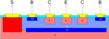
Location of the track resistances in the semiconductor of the bipolar transistor
Since the semiconductor material represents a resistance for the electrical current, this resistance must be represented in the form of the track resistance. A distinction is made between the emitter path resistance R E , the collector path resistance R C and the base sheet resistance R B .
- Emitter path resistance
- Due to the heavy doping and the low length-to-cross-section ratio of the emitter, R E only has a small amount. For small power transistors , R E is about 0.1 Ω to 1 Ω and for power transistors about 0.01 Ω to 0.1 Ω.
- Collector path resistance
- The collector path resistance is mainly caused by the weakly doped collector zone. In the case of low- power transistors , R C is approximately 1 Ω to 10 Ω and in the case of power transistors approximately 0.1 Ω to 1 Ω.
- Base resistance
- The base resistance is formed from the external base resistance R Be and the internal base resistance R Bi . The external base resistance occurs between the contact of the base and the active base zone, while the internal base resistance occurs across the active base zone between emitter and collector. With high currents, the internal base resistance has only a limited influence, as the current is concentrated in the base zone due to the current displacement . In addition, there is the early effect , which influences the thickness of the base zone. These effects are in constant q B summarized.
- The base resistance results from:

- For normal operation, by solving q B :

- In the case of small power transistors , R Be is approximately 10 Ω to 100 Ω and in the case of power transistors approximately 1 Ω to 10 Ω. R Bi is here about three to four times as large as R Be .
Substrate diode
Lateral integrated pnp transistor

Vertical integrated npn transistor
In the case of integrated transistors, vertical npn transistors between the substrate and collector, and lateral pnp transistors between the substrate and base, have a pn junction, the so-called substrate diode , due to the design - as shown in the adjacent figures . This substrate diode is described as a conventional pn diode using the Shockley formula . The reverse saturation current of the substrate diode I S, S is used for the reverse saturation current I S :
-
 (lateral)
-
 (vertical)
Since the substrate diode is usually not connected, no modeling is required. In the event of (faulty) wiring, however, a current can flow and must be taken into account in this case.
Modeling dynamic effects in the transport model
When controlling with sinusoidal or pulse-shaped signals, the dynamic behavior of the transistor must also be taken into account. For this, as with the diode , the blocking and diffusion capacitances occurring in the transistor are required.
Junction capacities
With a single bipolar transistor, two and with integrated transistors three junction capacitances occur. The emitter diode is characterized by the emitter junction capacitance . The collector diode is described by the collector junction capacitance , which is made up of the internal junction capacitance of the active zone and the external junction capacitance of the base connection . The proportions of the internal and external junction capacitance in the collector junction capacitance is represented by the parameter :


For single transistors, the factor is mostly between 0.5 and 1, which means that is. With integrated transistors, and thus .


In the case of integrated transistors, the junction capacitance of the substrate diode also occurs. In the case of integrated vertical npn transistors, this acts on the internal collector and in the case of integrated lateral npn transistors on the internal base . Therefore:


Diffusion capacities
Two diffusion capacitances occur in the transistor : the diffusion capacitance of the emitter diode and the diffusion capacitance of the collector diode . The emitter diffusion charge and the collector diffusion charge are stored in these . The diffusion charges result from the transport current that flows from the collector to the emitter ( see also: transport model ).


The time constants and are referred to as transit time . By differentiation arising from these equations, the diffusion capacity:


The diffusion capacitances and occur parallel to the junction capacitances and . In normal operation, the collector diffusion capacitance is very small due to the low internal base-collector voltage compared to the internal collector-junction capacitance and can therefore be neglected. can be described with a constant transit time as a result of neglecting , which is assumed.


If the transit current is small, the following applies if the transit current is large . In order to be able to represent this correctly, the equivalent circuit must be modeled precisely. An increase in gei large currents has the effect of a decrease in the cutoff frequencies and the switching speed of the transistor.


Due to the high current effect , the diffusion charge increases disproportionately. The transit time is therefore not constant and increases with increasing current. The early effect also has an effect , as it changes the effective thickness of the base zone and thus the charge stored in the base zone. However, since no precise description is possible with the parameters and , an empirically determined equation is used for the description:

Course of in double logarithmic representation

![\ tau _ {N} = \ tau _ {{0, N}} \, \ left [1 + x _ {{\ tau, N}} \, \ left (3 \, x ^ {2} -2 \, x ^ {3} \ right) \, 2 ^ {{\ frac {U _ {{B'C '}}} {U _ {{\ tau, N}}}}} \ right]](https://wikimedia.org/api/rest_v1/media/math/render/svg/ecb450c074ab3b46e1033b8dbd933853f0016ebe)
where the factor x for the polynomial is defined by the following equation:

In addition, the ideal transit time , the coefficient of the transit time , the transit time knee current and the transit time voltage . The coefficient of transit time here specifies how much at may increase:


Half of the maximum increase is obtained at :


It follows that if the voltage drops by the amount of the voltage , it only increases at half the speed. d. H. for the increase of is smaller by the factor .


Static small signal model
The static small-signal model describes the small- signal behavior at low frequencies and is therefore also referred to as a direct current small-signal equivalent circuit .
The linear small-signal model is created from the Gummel-Poon model through linearization in the operating point . The operating point is selected in a range in which the transistor should work after dimensioning. Usually this is normal operation, which is why models for normal operation are shown below. However, models for the other transistor operating modes can also be created using the same principles .
The linearization of the Gummel-Poon model takes place by omitting the capacitances - since these do not work with direct current - and neglecting the reverse currents - i.e. setting I B, I , I B, C and I D, S equal to zero.
 Static small signal model by neglecting capacities and reverse currents in the Gummel-Poon model
|
 Static small signal model after the linearization of I B and I C
|
Furthermore, the non-linear quantities and in the operating point A are linearized:


In practice, the track resistances are also not taken into account for further simplification. This gives the simplified static small-signal model . If the early effect is additionally neglected, an alternative type of representation of this simplified model is obtained, which is created from the simplified static small-signal model by linearization. However, due to the neglected early effect, the alternative display type can only be used in exceptional cases, as the calculation based on this simplification usually leads to unusable results. In the literature one can also often find a representation with an additional resistance between base and collector, which results from the linearization of the collector-base diode from the Ebers-Moll model, but does not serve to model the Early effect.

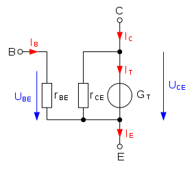 Simplified static small signal model with neglected rail resistances
|
 Reshaped, simplified static small-signal model with additional neglect of the early effect
|
The equations apply here


Dynamic behavior models
Gummel Poon model
The Gummel-Poon model , named after its intellectual fathers Hermann Gummel and HC Poon, is the complete model of a bipolar transistor and is used for circuit simulation - for example in PSpice . It is based on the transport model and models all static and dynamic effects in it. The symbols are listed at the beginning of the article.

Gummel-Poon model of an npn bipolar transistor
If some values are not specified in the data sheet of the transistor, standard values are used (e.g. in PSpice). The following standard values are used in PSpice:
Standard values of the Gummel-Poon model in PSpice
| parameter
|
I S
|
B N
|
B I
|
n E
|
n C
|
x T, I
|
f p
|
U diff, E , U diff, C , U diff, S
|
m S, E , m S, C
|
x CSC
|
I S, S , I S, E , I S, C ,
R B , R C , R E ,
C S0, E , C S0, C , C S0, S ,
τ 0, N , τ 0, I , x τ, N , x T, B ,
m S, S , I τ, N
|
I K, N , I K, I ,
U A, N , U A, I , U τ, N
|
| default value
|
10 −16 A
|
100
|
1
|
1.5
|
2
|
3
|
0.5
|
0.75 V
|
333 · 10 −3
|
1
|
0
|
∞
|
A standard value of 0 or ∞ means that the corresponding parameter is set in such a way that this parameter has no influence on the calculation and is not modeled in this way.
Values for the Gummel-Poon model of selected individual transistors
| parameter
|
PSpice
name
|
BC547B
|
BC557B
|
BUV47
|
BFR92P
|
| I S
|
IS |
7 f A
|
1 fA |
974 fA |
0.12 fA
|
| B N
|
BF |
375 |
307 |
95 |
95
|
| B I
|
BR |
1 |
6.5 |
20.9 |
10.7
|
| I S, E
|
ISE |
68 fA |
10.7 fA |
2.57 pA |
130 fA
|
| n E
|
NE |
1.58 |
1.76 |
1.2 |
1.9
|
| I K, N
|
IKF |
82 mA |
92 mA |
15.7 A |
160 mA
|
| U A, N
|
VAF |
63 V
|
52 V |
100 V |
30 V
|
| R Be
|
RBM |
10 Ω
|
10 Ω |
100 mΩ |
6.2 Ω
|
| R Bi
|
- |
0 |
0 |
0 |
7.8 Ω
|
| - |
RB |
10 Ω |
10 Ω |
100 mΩ |
15 Ω
|
| R C
|
RC |
1 Ω |
1.1 Ω |
35 mΩ |
140 mΩ
|
| C S0, E
|
CJE |
11.5 p F
|
30 pF |
1.093 nF |
1 fF
|
| U diff, E
|
VJE |
500 mV |
500 mV |
500 mV |
710 mV
|
| m S, E
|
MJE |
672 · 10 −3
|
333 · 10 −3 |
333 · 10 −3 |
347 · 10 −3
|
| C S0, C
|
CJC |
5.25 pF |
9.8 pF |
364 pF |
649 ff
|
| U diff, C
|
VJC |
570 mV |
490 mV |
500 mV |
850 mV
|
| m S, C
|
MJC |
315 · 10 −3
|
332 · 10 −3
|
333 · 10 −3 |
401 · 10 −3
|
| x CSC
|
XCJC |
1 |
1 |
1 |
130 · 10 −3
|
| f p
|
FC |
500 · 10 −3 |
500 · 10 −3 |
500 · 10 −3 |
500 · 10 −3
|
| τ 0, N
|
TF |
410 p s
|
612 ps |
51.5 ns |
27 ps
|
| x τ, N
|
XTF |
40 |
26th |
205 |
380 · 10 −3
|
| U τ, N
|
VTF |
10 V |
10 V |
10 V |
330 mV
|
| I τ, N
|
ITF |
1.49 A |
1.37 A |
100 A |
4 mA
|
| τ 0, I.
|
TR |
10 ns |
10 ns |
988 ns |
1.27 ns
|
| x T, I
|
XTI |
3 |
3 |
3 |
3
|
| x T, B
|
XTB |
1.5 |
1.5 |
1.5 |
1.5
|
Remarks:
-
↑ a b c d e f g h i j k l m n o corresponds to the standard value
-
↑ a b c d e f g h i Value only given in general. Inaccuracies occur at high frequencies.
This is taken into account in the transistor noise. Otherwise the correct value would have to be determined by measuring the individual component.
-
↑ a b R Bi is not specified explicitly in PSpice. Instead, R B is given as R B = R BM + R Bi = R Be + R Bi .
|
In addition, some other effects are taken into account in PSpice, which are described in the PSpice reference manual, for which the model used in PSpice has been extended accordingly.
Dynamic small signal model

Dynamic small signal model of the bipolar transistor
If the complete static small-signal model is expanded to include the junction and diffusion capacitances, the dynamic small-signal model is obtained .
The emitter capacitance is made up of the emitter-junction capacitance and the diffusion capacitance for normal operation :


The internal collector capacitance corresponds to the internal collector-junction capacitance , since the internal diffusion capacitance is negligibly small because of :


The external collector capacitance and the substrate capacitance correspond to the respective junction capacitances, whereby the substrate capacitance can naturally only be found with integrated transistors:


Simplified dynamic small signal model of the bipolar transistor

In practice, the emitter resistance and the collector resistance are mostly neglected, while the base resistance can only be neglected in exceptional cases, since the base resistance has a strong influence on the dynamic behavior. In addition, in practice the internal and external collector capacitance - with the exception of integrated transistors with a predominantly external collector capacitance - are combined as internal collector capacitance . This gives the simplified dynamic small-signal model:

Limit frequency in small-signal operation
With the help of the small-signal model , the frequency responses of the small-signal current gains and , as well as the transmittance , can be determined mathematically. The respective cut-off frequencies , , as well as the transit frequency provide a measure of the switching speed and bandwidth of the transistor is this true of context.


If the emitter- connected transistor is operated with a current source - or with a source with an internal resistance of - it is called current control . In this case, the limit frequency is limited by the β-limit frequency .


If, on the other hand, the transistor is operated in an emitter circuit with a voltage source - or with a source with an internal resistance of -, one speaks of voltage control . In this case, the limit frequency is limited by the slope limit frequency .

It follows that with voltage control, a higher cutoff frequency and thus a higher bandwidth can be achieved. This also applies to the collector circuit . However, the largest bandwidth is achieved by the basic circuit in which the condition generally applies and there is thus a current control and the bandwidth is limited upwards by the α cut-off frequency .

The bandwidth of the circuit is also dependent on the operating point. In the emitter circuit with current control and in the basic circuit, the maximum bandwidth is obtained by setting the collector current so that the transit frequency reaches the maximum value. In the case of the emitter circuit with voltage control, there is a more complicated relationship, since the slope frequency decreases with increasing collector current , but at the same time the circuit of the collector circuit becomes lower and the output-side bandwidth of the circuit is increased.


|
|

Dependence of the transit frequency of a transistor on the collector current
|
The transition frequency and the output capacity in base circuit ( o utput , grounded b ase , o pen emitter ) is specified in the data sheet of the transistor. This corresponds to the collector-base capacity . This results in:


literature
- Ulrich Tietze, Christoph Schenk, Eberhard Gamm: Semiconductor circuit technology. 12th edition. Springer, 2002, ISBN 3-540-42849-6 .
- Paul R. Gray, Paul J. Hurst, Stephen H. Lewis, Robert G. Meyer: Analysis and Design of Analog Integrated Circuits . Wiley, 2001, ISBN 0-471-32168-0 .
-
Simon M. Sze : Physics of Semiconductor Devices . Wiley 1981, ISBN 0-471-05661-8 .
- Hans-Martin Rein, Roland Ranfft: Integrated bipolar circuits . Springer, 1980, ISBN 3-540-09607-8 .
- Giuseppe Massobrio, Paolo Antognetti: Semiconductor Device Modeling with SPICE . McGraw-Hill Professional, 1998, ISBN 0-07-134955-3 .
Individual evidence
-
↑ Data sheet of the transistor BC547B
-
↑ Data sheet of the transistor BC557B
-
↑ Data sheet of the transistor BUV47
-
↑ Data sheet of the transistor BFR92P
-
↑ MicroSim: PSpice A / D. Reference Manual. MicroSim Corporation, 1996.


.svg)
.svg)


.svg)
.svg)


