
Epitaxial transistor
As Epitaxialtransistor , even epitaxial transistor or Epitaxietransistor , is generally a transistor with one or more epitaxially referred deposited layers. As a rule, however, a single bipolar transistor in mesa or planar technology (epitaxial mesa transistor and planar transistor ) is referred to, as it was first presented in 1960 and, due to its electrical properties, quickly became one of the most important and most widely used transistors in the early 1960s wrapped.
History and background
After the first practical implementation of a bipolar transistor in 1949, numerous further developments with improved properties were presented in the 1950s. Back then, before the invention of the integrated circuit , only single or Darlington transistors were manufactured. Milestones were the invention of the mesa and planar transistors ( Jean Hoerni , 1959), which quickly became the common designs for bipolar transistors around 1960 due to their good electrical properties. Both were usually vertical bipolar transistors in which the base and emitter regions were diffused into one surface of an n- or p-doped substrate (usually from the gas phase ). The collector connection was attached to the back of the substrate. The comparatively wide (approx. 0.2 mm) collector zone is used for the mechanical stability of the "chip", but has disadvantages in terms of switching behavior, e. B. longer switch-off times due to charge storage in the large collector zone.
As early as 1954, James Early proposed a transistor with a low-doped collector zone. At that time, however, this could not be implemented in practice, since, for example, only a more highly doped zone could be generated through the usual diffusion and the use of a less doped substrate would have prevented an improvement in the electrical properties. That changed with the development of epitaxial deposition (as early as 1951 by Gordon Teal and Howard Christensen ). It was now possible to deposit a lightly doped layer on a differently doped substrate. The first epitaxial transistor (made of germanium ) was presented by a group of researchers led by Ian Ross ( Bell Labs ) at the Solid-State Device Research Conference (SSDRC) in June 1960. Numerous manufacturers took over the idea for transistors made of germanium and, above all, of silicon , as they are a good alternative to the micro alloy transistors (MAT) and micro alloy diffusion transistors (MADT) from Philco Corporation saw. These included Fairchild Semiconductor (2N914), Rheem (2N297), Sylvania , Motorola and Texas Instruments .
The development was so significant that the much more important development of the metal-oxide-semiconductor field effect transistor (MOSFET) by Martin Atalla and Dawon Kahng , which was also presented at the SSDRC in 1960, hardly received any attention there.
Structure and properties
In contrast to the diffusion transistor mentioned (in mesa or planar technology), in the case of the epitaxial transistor, a lightly doped layer of the same doping type (n- or p-doped) is epitaxially deposited on a highly doped (and thus low-resistance) substrate. This epitaxial layer serves as an “active” collector zone and can be kept comparatively thin (approx. 0.01 mm). The two-layer collector structure results in a relatively low collector rail resistance, which leads to better switching behavior and higher gain. The base and emitter regions are in turn diffused into this epitaxial layer, cf. Pictures below.
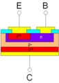
Schematic structure of a pnp-doped bipolar transistor in epitaxial planar technology

Schematic structure of an npn-doped bipolar transistor in epitaxial planar technology

Practical construction of an npn-doped bipolar transistor in epitaxial planar technology
Another form of the epitaxial transistor is the transistor with a grown base introduced in 1963, originally English. epitaxial base transistor . A lightly doped layer of the opposite doping type (n- or p-doped), which forms the base zone, is epitaxially deposited on a heavily doped substrate. Then only the diffusion of the emitter zone into this layer takes place. The advantage of this structure is the significantly more uniform doping of the base (during the epitaxial deposition). In comparison with transistors with a diffused base, the base-emitter breakdown voltage can thus be increased. In addition, this design allowed a higher current gain.
Web links
- 1960 - Epitaxial Deposition Process Enhances Transistor Performance. In: computerhistory.org. Computer History Museum, accessed July 19, 2015 .
Individual evidence
- ^ Rudolf F. Graf: Modern Dictionary of Electronics . Newnes, 1999, ISBN 0-7506-9866-7 , p. 262 ( limited preview in Google book search).
- ↑ a b c Martin Kulp: Tube and transistor circuits . Vandenhoeck & Ruprecht, 1970, ISBN 3-525-42803-0 , p. 456 ( limited preview in the Google book search).
- ↑ a b c Dermot Roddy: Introduction to Microelectronics . Elsevier, 2013, ISBN 978-1-4831-5539-5 , p. 38 ( limited preview in Google book search).
- ^ RL Petritz: Contributions of Materials Technology to Semiconductor Devices . In: Proceedings of the IRE . tape 50 , no. 5 , 1962, pp. 1025-1038 , doi : 10.1109 / JRPROC.1962.288004 .
- ^ HH Loor, H. Christensen, JJ Kleimock, HC Theure: New advances in diffused devices . IRE-AIEE Solid-State Device Research Conference, Pittsburgh, PA, June 1960 (conference contribution).
- ^ Bo Lojek: History of Semiconductor Engineering . Springer Science & Business Media, 2007, ISBN 978-3-540-34258-8 , p. 116 ( limited preview in Google book search).
- ^ A b Peter Robin Morris: A History of the World Semiconductor Industry . IET, 1990, ISBN 0-86341-227-0 , p. 40 ( limited preview in Google book search).