Nano emboss lithography
The nano-imprint lithography ( English lithography nanoimprint , short NIL) is a nanolithography method for inexpensively producing nanostructures by means of a nano-structured stamp . Monomers or polymers that have to harden after embossing are often used as positive . Nano-embossed lithography is used in the manufacture of electronic and opto-electronic components.
history
The technique of nano-embossed lithography was invented at the beginning of the 1990s by Walter Bacher's group at the Institute for Microstructure Technology at the Karlsruhe Research Center and could already be used for the production of nanostructures at that time. Since then, the technology has been the subject of current research and, according to the International Technology Roadmap for Semiconductors , is intended for chip production in 20 nm from 2014 . In 2003, Technology Review listed nano-embossed lithography as "one of the ten emerging technologies that will change the world". Since 2006 there have been stamps for the production of three-dimensional nanostructures with a vertical resolution in the sub- nanometer range, i.e. H. less than a nanometer.
Manufacturing processes
Nanoimprint
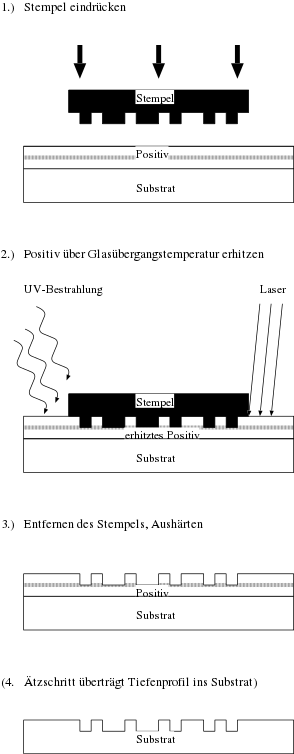
For the production of nanostructures by means of nano-embossed lithography you need a positive, usually a monomer or polymer, as well as a nano-structured stamp. The stamp itself can in turn be produced by nanolithography or etching. The positive is applied to a substrate and then heated above the temperature of the glass transition , i. that is, it becomes liquid before the stamp is pressed in. In order to achieve controllable (and short-term) heating, lasers or UV light are often used, which is particularly necessary in several process steps during production, since otherwise the negative will also melt again.
Due to the viscosity of the positive when heated, the gaps in the stamp are completely filled with it. After cooling, the stamp is removed again. This means that the adhesion between positive and stamp is an important parameter (in addition to temperature and press-in pressure). A process was developed at the University of Kassel in which the stamps are coated with a monomolecular coating so that they can be removed more easily from the material.
If the embossed depth profile is to be transferred into the substrate or the actual layer, the positive must be etched away beforehand (step 4 in the figure opposite).
With nano-embossed lithography with UV light, lower contact pressures can be used, and the process can also take place at room temperature .
stamp
The structuring of the stamps for lithography can again be done with nanoimprint, but also with other nanolithography processes. Glass or light-transparent plastics are used as materials. Due to the small structural sizes of the stamp, an atomic force microscope can not be used for its quality control , since the image sizes are not correctly reproduced due to the size of the measuring tip. Instead, the stamp can be examined with a scanning electron microscope , which, however, requires an electrically conductive coating (e.g. indium tin oxide ) on the stamp.
Applications
Nano-embossed lithography is used to produce two- and three-dimensional organic or semiconductor nanostructures for optics, electronics, photonics and biology. Applications in optics and photonics are optical filters , polarizers , micromirror arrays , non-reflective structures or photonic circuits . Quantum wires and dots are of interest for optical semiconductor elements such as lasers or diodes. Electronic circuits such as MOSFETs , organic TFTs or individual electron storage devices can also be implemented more cheaply and easily than with techniques such as electron beam or EUV lithography . In biology, nanostructures are u. a. interesting for the transport of liquids or the separation of biomolecules.
Advantages and disadvantages
Nanoimprint can be used to inexpensively manufacture nanostructures, e.g. B. integrated circuits in silicon technology, with a resolution below the diffraction limit of light can be used. The production of multi-layer structures is also possible with this technology.
During the manufacturing process, however, the temperature and pressure resistance of the materials used must be taken into account.
Web links
Individual evidence
- ^ A. Michel, R. Ruprecht, M. Harmening, W. Bacher: Impression of microstructures on processed wafers. KfK report 5171, 1993 (at the same time, dissertation by A. Michel, University of Karlsruhe, Institute for Microstructure Technology 1992).
- ↑ Brief description of "NanoImprint Technology"
- ↑ International Technology Roadmap for Semiconductors 2009: Lithography ( Memento of the original from June 12, 2010 in the Internet Archive ) Info: The archive link was automatically inserted and not yet checked. Please check the original and archive link according to the instructions and then remove this notice. (PDF; 301 kB)
- ↑ a b c 10 Emerging Technologies That Will Change the World . Technology Review, February 2003, page 8.
- ↑ a b Hessen Nanotech News 2/2008 ( memento of the original from October 19, 2011 in the Internet Archive ) Info: The archive link was automatically inserted and not yet checked. Please check the original and archive link according to the instructions and then remove this notice.
- ↑ Sergiy Zankovych, Nanoimprint lithography as an alternative fabrication technique: towards applications in optics . Bergische Universität Wuppertal, 2004, doctoral thesis, urn : nbn: de: hbz: 468-20040385 .
- ^ A b D. J. Resnick et al: Imprint lithography for integrated circuit fabrication . In: Journal of Vacuum Science & Technology B: Microelectronics and Nanometer Structures . tape 21 , no. 6 , 2003, p. 2624-2631 , doi : 10.1116 / 1.1618238 .
- ↑ a b High-resolution 3D NanoImprint stamp and NanoImprint technology
- ↑ a b Stephen Y. Chou, Peter R. Krauss, Preston J. Renstrom: Nanoimprint lithography . In: Journal of Vacuum Science Technology B: Microelectronics and Nanometer Structures . tape 14 , no. 6 , November 1996, pp. 4129-4133 , doi : 10.1116 / 1.588605 .
