
Electron beam lithography
The electron beam lithography (ESL, English electron beam lithography often referred to as e-beam lithography hereinafter) is in the micro and semiconductor technology, a special method for structuring a electron -sensitive layer (engl. Resist , in analogy to the photolithography and photoresist called). The process belongs to the group of next-generation lithography and is closely related to ion beam lithography . "Exposure" to an electron beam chemically changes the resist so that it can be locally dissolved (development) and a structured resist layer is created. The structure can then be transferred to a layer of another material, e.g. B. by etching an underlying layer or by selective deposition of a material on the resist. The main advantage of the process is that structures with significantly smaller dimensions (in the nanometer range) can be produced than with photolithography.
The process is of great importance in the production of microelectronic circuits for modern electronic devices and is used above all in the production of the photomasks used in photolithography . However, it can also be used as a maskless lithography process for structuring layers or wafers in prototype or small series production. Electron beam lithography is also traded in large-scale production as a successor to today's (as of 2011) photolithography based on excimer lasers . The long process times of current technologies in which the electron beam is scanned over the substrate, for example, are not economical and also lead to technical problems, e.g. B. Electron beam instabilities.
Energy release from electrons in matter
scattering
Electrons are particles with a relatively low mass compared to atomic nuclei . If electrons from an incident beam (primary electrons) hit the resist with high energy (typically 10–50 keV), they experience both forward and backscattering in the material . Forward scattering means a deflection of the electrons of less than 90 ° in the direction of incidence. The scattering causes, among other things, a widening of the beam diameter and thus leads to an effective deterioration in the resolution, but this is less than that caused by the generation of secondary electrons . Sometimes the primary electrons are scattered at an angle greater than 90 degrees, that is, they are not scattered further in the substrate. These electrons are backscattered electrons (engl. Backscattered electrons ) referred to and have the same effect as long-range lens scattering effects (engl. Lens flare ) of the optical projection systems. A sufficiently large dose of backscattered electrons can lead to a complete exposure of an area significantly larger than the beam cross section in the focus.
Generation of secondary electrons
In addition to the elastic scattering in the resist or substrate, the primary electrons experience inelastic scattering or collisions with other electrons (e.g. the electrons of the lattice atoms) when they enter or pass through a material such as the resist . In such a collision the primary electrons lose energy through a momentum transfer from the incident electron to the other electron and can be described by the relationship , whereby the distance between the electrons is closest and the speed of the incident electron. The energy that is transferred by the collision can be described in terms of the context , where the mass of the electron, the elementary charge and the electron energy, corresponds to. By integrating over all values of between the lowest binding energy and the incident energy, the result is that the total cross-section of a collision is inversely proportional to the incident energy and proportional to . In general, the result is essentially inversely proportional to the binding energy.


By using the same integration approach , but over the range to , by comparing the cross-sections, one obtains that half of the inelastic collisions of the incident electrons generate further electrons with a kinetic energy greater than . These electrons, called secondary electrons, are also able to break chemical bonds (with binding energy ), even at some distance from the original collision. In addition, they can generate electrons with lower energy, which means that an electron cascade is created . It is therefore important to consider the contribution of the secondary electrons to the propagation of the energy input.


Resolving power
In contrast to optical lithography, electron beam lithography is practically not limited by the wavelength of the particles used. The wavelength of electrons with an energy of approx. 25 keV is around 8 picometers, which corresponds to around one twelfth of the diameter of the hydrogen atom . The resolution is therefore more dependent on the beam diameter used, which in turn is limited by the electron source, the aberration of the electron optics and the interactions in a highly collimated electron beam. With today's electron optics, electron beams with cross-sections of a few nanometers can be generated. However, the practical limit of resolution is not exclusively determined by the beam diameter, but also by forward scattering in the resist and, above all, the secondary electrons moving in the resist. Forward scattering can be reduced by using higher electron energies or thinner resist layers, but the generation of secondary electrons is inevitable. The distance traveled by a secondary electron is not a generally calculable value, but a statistical parameter that can be determined using many experiments or Monte Carlo simulations with an energy of less than 1 eV. This is necessary because the peak value in the energy distribution of the secondary electrons is well below 10 eV. Repeatability and control of the practical resolution limit often require the consideration of influences that are not related to the formation of the image, e.g. B. Resist Development and Intermolecular Forces.
Writing time
The minimum exposure time for a given area at a given radiation dose is described by the following formula:


For example, the minimum exposure time for an area of 1 cm², a dose of 10 −3 C / cm² and a beam current of 10 −9 A is approx. 10 6 s (approx. 12 days). This minimum writing time does not include the time for moving the substrate holder, the beam is masked out and other possible technical corrections and adjustments during writing. In order to cover the 700 cm² surface of a 300 mm silicon wafer, the minimum writing time would be extended to 7 · 10 8 seconds, about 22 years. It is clear that the throughput is a serious limitation for electron beam lithography, especially when exposing dense structures over a large area. Direct writing methods with only one beam are therefore not suitable for high volume production. Because to expose a pattern with a sub-100 nm resolution with electron beam lithography on a single wafer would normally take several days, compared to today's 193 nm photolithography systems need less than a minute for the same task.
Proximity effect
The smallest structures produced by electron beam lithography, since the production of densely standing structures (mostly lines) by the proximity effect (eingedeutscht of Engl. Generally isolated structures effect proximity : dt. , Proximity effect ") is difficult. The proximity effect describes the crosstalk of electrons during exposure, that is, electrons that were "intended" to expose a certain structure outshine the intended area and contribute to the exposure of adjacent areas. This leads to an enlargement of the written structures, effectively expands their image and leads to a decrease in contrast, i.e. H. the difference between maximum and minimum intensity in an area. Therefore, the exposure or resolution of dense structures is more difficult to control. With most resists it is therefore difficult to produce lines and trenches smaller than 25 nm; the lower limit is currently 20 nm.
The main cause of the proximity effects is the scattering of electrons due to the electrical interaction of the negatively charged electrons with one another. However, the problem can be reduced by a previously calculated correction of the exposure function. It enables a dose distribution as close as possible to the desired dose


Charging
If a high-energy electron beam hits a substrate, it stops some of the electrons. Since electrons are charged particles, they tend to negatively charge the substrate if they are not quickly dissipated towards mass. For substrates with low conductivity, such as a silicon wafer, this is usually not a problem. The situation is different with non-conductive or poorly conductive substrates, such as the quartz substrates used for photomasks. A negative charge within the substrate is often accompanied by a positive counter charge on the surface, which is mainly caused by secondary electron emission into a vacuum. The range for the emission of low-energy secondary electrons (the largest component of free electrons in the resist-substrate system), which can contribute to charging, is between 0 and 50 nm below the surface. The charging of the resist or the substrate is generally not repeatable and therefore difficult to compensate. Positive charges are less bad than negative charges because the latter can deflect the electron beam from the desired position during exposure.
Similar effects also occur in scanning electron microscopy, where they lead to a loss of contrast and lower resolution. There you can make do with the application of a thin conductive layer on the sample. In ESL, such conductive layers above or below the resist are generally of limited use, since high-energy (50 keV or more) electron beams can pass through the layers relatively unhindered and continue to accumulate in the substrate. In the case of low-energy rays, on the other hand, it is quite effective and useful.
Electron beam lithography systems
Electron beam lithography systems essentially consist of an electron source, an electron-optical system and the deflection or projection unit (focusing). Due to the linear arrangement of the components, the entire structure is also referred to as a column.
Systems with low resolution can use hot cathodes , mostly based on lanthanum hexaboride (LaB 6 ). Systems with higher resolution, on the other hand , require field emission sources such as heated W / ZrO 2 for lower energy consumption and improved intensity. Thermal field emission sources are preferred to cold emission sources despite their somewhat larger beam size, because they offer better stability when writing over a longer period of time (several hours).
Special system components are required for the concentration and focusing of the electron beams, which are often referred to as lens systems in analogy to optics. Both electrostatic and magnetic lenses can be used in ESL systems. However, electrostatic lenses show greater aberration and are therefore not suitable for fine focusing. Because currently there are no techniques for the production of achromatic electron beam lenses, so that electron beams with an extremely narrow energy dispersion are required for extremely fine focusing.
Electrostatic systems are typically used for very small deflections of the electron beam; larger beam deflections require electromagnetic systems. Because of the inaccuracy and the finite number of exposure steps, the exposure field is of the order of 100 to 1000 µm. Larger samples require a movement of the substrate support ( stage or chuck ) , which must meet particularly high requirements with regard to the juxtaposition of the samples and the alignment of a sample on one level compared to the previous level, cf. Overlay (semiconductor technology) .
The ESL systems used for commercial applications are dedicated, such as photomask manufacturing, and are very expensive (over $ 4 million). In contrast, devices for research applications are often modified electron microscopes that have been converted into an ESL system at a comparatively low cost (less than 100,000 USD). This is also reflected in the achievable results, for example structure sizes of 10 nm and smaller could be mapped with the dedicated systems. With research devices based on electron microscopes, on the other hand, only sizes of approx. 20 nm can be displayed.
Electron beam paints (resists)
Short-chain and long-chain polymethyl methacrylates (PMMA resist, sensitivity at 100 keV approx. 0.8–0.9 C / cm²) are one of the first and still used today . This is usually a one-component paint. On the other hand, as with normal photoresists, there are also multi-component lacquers in which, in addition to the electron-sensitive component, substances are added that ensure a stronger crosslinking of the lacquer after exposure (so-called chemically reinforced lacquers).
Furthermore, there is a search for electron-sensitive or chemically more stable lacquers in order to enable shorter exposure times, for example. The electron-sensitive paints include u. a. Hydrogen silsesquioxane (engl. Hydrogen silsesquioxane , HSQ, about 1 C / cm² @ 100 keV) or calixarenes (about 10 C / cm² and greater @ 100 keV). Unlike PMMA, these two resists are negative resists , which means that the exposed areas remain on the wafer after the resist has been developed.
Procedure
ESL systems include both maskless and maskless methods. Both groups of procedures can be broken down into various sub-techniques.
The maskless methods, i.e. direct writing with a guided electron beam, can be classified according to both the beam shape and the strategy of beam deflection. Older systems use Gaussian- shaped electron beams that are guided over the substrate (raster mode). Newer systems use shaped beams, i.e. beams on which a desired geometric cross-section has been imprinted via a mask, and their deflection to different positions in the "text field" (vector scan mode).
The mask-based processes are similar to conventional photolithography. In ESL, too, there are specific proximity irradiation techniques such as 1: 1 projection or projections in which the structures of the mask are reduced.
Maskless techniques
When the information is written directly into the resist, an electron beam is imaged without a mask. For this purpose, the beam is guided over the substrate in accordance with the desired mask structure. The necessary deflection is achieved through electrostatic interactions between the electrons.
Raster and vector scan principle
With the raster scan principle, the electron beam is guided line by line over the exposure field. This is comparable to the beam guidance in a tube monitor or a scanning electron microscope. The structures are exposed by specifically switching the electron beam on and off. The XY table of the substrate support is usually moved continuously.
In contrast to this, with the vector scan principle the beam is specifically deflected onto the structure to be exposed in the exposure field and written there in a meandering or spiral-shaped movement of the electron beam. After all structures in the deflection field have been exposed, the XY table moves to the next position, similar to the step-and-repeat process used in today's photolithography systems. This principle has a clear advantage in terms of process time, especially in less structured areas.
Beam shape
Both the raster and the vector scan principle can use electron beams of different shapes. In terms of energy distribution (in the beam cross-section), they are divided into the following types:
- solid-shaped beams (engl. fixed-shaped beam )
- round rays
- Gaussian round-beam , Gaussian energy distribution
- square-shaped beam (engl. square-beam )
- round spot with uniform energy distribution ( round-beam )
- variably -shaped beam , these are mostly square and triangles of different sizes and shapes
The beam shape is generated via an aperture or structured aperture plates. The latter can be thought of as simple pinhole diaphragms with a certain geometry.
Mask-based techniques
The maskless techniques have a major disadvantage, the long write time per wafer. In order to make the ESL attractive for large-scale production, alternative techniques were developed, e.g. B. Multiple beam recorder. Mask-based techniques, such as those already used in conventional photolithography, are also of interest. Electron beams offer a significant advantage over exposure to light; due to their very short wavelength ( De Broglie wavelength ), they do not show any practically relevant diffraction effects that would interfere with the transfer of structures from a mask into the resist.
The exposure takes place via a shadow projection of the mask structures with the help of a parallel electron beam. The masks are either transmission masks in which the structures have been " punched out" ( stencil mask ), or masks in which an absorbing layer has been applied and structured on an electron- beam transparent substrate, similar to common photo masks. After exposure, the exposure field is shifted to the next exposure position on the wafer or substrate using the step-and-repeat method.
SCALPEL
SCALPEL ( Scattering with Angular Limitation Projection Electron-beam Lithography ) is another mask-based technique that uses a scatter mask on a film that is transparent to electrons. Similar to conventional photolithography, certain parts of the electron beam are shaded by the mask. A scattering layer is used for this purpose, which strongly deflects the electrons that strike. They are then masked out via an aperture diaphragm. The advantage of a scattering layer over absorption of the electrons is, on the one hand, the significantly lower charge and, on the other hand, less heating of the mask.
Example of a process flow
The following example uses the illustrations to show how electron beam lithography can be used to create a metal nanobridge for certain fracture contact experiments. An elastic substrate made of sheet bronze is required for the experiment, as well as a free-standing metal bridge with a predetermined breaking point that slowly tears when the substrate is bent. The structure is used in basic research to create one-atom contacts. In this application, scanning electron beam lithography is particularly suitable for production, since only a few samples are required as research objects and the required structure size with a 100 nm wide narrow point is normally not achieved with optical lithography processes.

Step 1: prepare the bronze substrate.

Step 3: Applying a soft electron beam lacquer as a buffer layer (spin coating + drying).

Step 4: Application of a hard PMMA lacquer as a vapor mask (spin coating + drying).

Step 5: Exposure with the electron beam of a scanning electron microscope ( SEM ).

Step 6: Developing in a developer liquid that dissolves the exposed areas (positive varnish).

Step 7: vapor deposition with metal, e.g. B. aluminum . The buffer layer leads to well-defined metal edges without touching the paint.

Step 9: Exposing the nanobridge by partially removing the sacrificial layer in the reactive ion plasma ( RIE ).
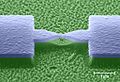
Finished aluminum nano-bridge on the polyimide base, viewed in the SEM (artificially colored).


Defects
Despite the high resolution of electron beam lithography, the generation of defects is often not considered by users. The defects that occur can be divided into two categories: data-related and physical defects.
Data-related defects can in turn be divided into two subgroups. Blanking or deflection errors occur when the electron beam is not deflected properly. On the other hand, shaping errors occur in systems with variable beam shape when the wrong shape is projected onto the sample. These errors can originate either from the electronic-optical control hardware or the input data. As can be expected, larger amounts of data are more prone to data-related defects.
Physical defects are more diverse and include effects such as the electrostatic charging of the sample (negative or positive), backscattering of the electrons, dose errors, fogging (long-range reflections of backscattered electrons), outgassing of the resist, contamination and beam expansion. Since the time for direct writing can easily take several hours (even over a day), random errors are more likely to occur. Again, larger amounts of data are more prone to defects.
Future developments
In order to solve the problems associated with secondary electron generation, it will become essential to use low energy electrons for the exposure of the resist. The energy of the electrons should ideally be of the order of just a few electron volts. This has already been shown in a study with an ELS system based on a scanning tunneling microscope. It was shown that electrons with energies lower than 12 eV can penetrate a 50 nm thick polymer photoresist. The disadvantage of using low-energy electrons is that it is difficult to prevent the electron beam from spreading in the photoresist. In addition, the design of electron beam systems for low beam energies and high resolution is difficult, since the Coulomb repulsion between the electrons is becoming more important.
An alternative is the use of extremely high energies (at least 100 keV) in order to achieve material removal by sputtering. This phenomenon has often been observed in transmission electron microscopy. However, this is a very inefficient process due to the inefficient transmission of the pulses from the electron beam to the material. This results in a slow process with much longer exposure times than conventional electron beam lithography. In addition, high radiation energies can damage the substrate.
In order to achieve a shortened exposure time and thus an economical throughput of at least 10 wafers per hour in the production of microelectronic circuits, approaches have been researched in which several electron beams ( multi-beam lithography ) are used simultaneously. With such multi-beam recorders, 10,000 and more beams should allow process times of well under an hour for the exposure of a 300 mm wafer.
See also
literature
- MA McCord, MJ Rooks: Chapter 2 . In: SPIE Handbook of Microlithography, Micromachining and Microfabrication 2000.
- DM Tennant, AR Bleier: Electron Beam Lithography of Nanostructures . In: Gary Wiederrecht (Ed.): Handbook of nanofabrication . Academic Press, 2010, ISBN 978-0-12-375176-8 , pp. 121-148 .
Web links
- Electron-beam lithography (PDF; 0.5 MB) at Cornell
Individual evidence
- ^ MA McCord, MJ Rooks: Chapter 2 . In: SPIE Handbook of Microlithography, Micromachining and Microfabrication 2000.
- ↑ L. Feldman, J. Mayer: Fundamentals of Surface and Thin Film Analysis . 1986, ISBN 0-13-500570-1 , pp. 130-133 .
- ↑ TO Broers, ACF Hoole, JM Ryan: Electron beam lithography - Resolution limits . In: Microelectronic Engineering . tape 32 , no. 1-4 , 1996, pp. 131-142 , doi : 10.1016 / 0167-9317 (95) 00368-1 .
- ^ H Seiler: Secondary electron emission in the scanning electron microscope . In: Journal of Applied Physics . tape 54 , no. 11 , 1983, pp. R1-R18 , doi : 10.1063 / 1.332840 .
- ↑ JA Liddle, GM Gallatin, LE Ocola, others: Resist requirements and limitations for nanoscale electron-beam patterning . In: Mat. Res. Soc. Symp. Proc. tape 739 , no. 19 , 2003, p. 19-30 , doi : 10.1557 / PROC-739-H1.5 .
- ↑ a b Gary Wiederrecht: Handbook of Nanofabrication . Academic Press, 2009, ISBN 0-12-375176-4 , pp. 131-133 .
- ↑ Hans Weinerth: Lexicon Electronics and Microelectronics . Springer, 1993, ISBN 978-3-540-62131-7 , pp. 245 .
- ↑ Lloyd R. Harriott: Scattering with angular limitation projection electron beam lithography for suboptical lithography . In: Journal of Vacuum Science & Technology B: Microelectronics and Nanometer Structures . tape 15 , no. 6 , 1997, pp. 2130 , doi : 10.1116 / 1.589339 .
- ↑ Ulrich Hilleringmann: silicon semiconductor technology . Vieweg + Teubner, 2004, ISBN 978-3-519-30149-3 , pp. 54-56 .
- ↑ JM Ruitenbeek, A. Alavarez, I. Pineyro, C. Grahmann, P. Joyez, MH Devoret, D. Esteve; C. Urbina: Adjustable nanofabricated atomic size contacts . In: Review of Scientific Instruments . tape 67 , no. 1 , 1996, p. 108-111 , doi : 10.1063 / 1.1146558 .
- ^ Christie RK Marrian: Electron-beam lithography with the scanning tunneling microscope . In: Journal of Vacuum Science & Technology B: Microelectronics and Nanometer Structures . tape 10 , no. 6 , 1992, pp. 2877-2881 , doi : 10.1116 / 1.585978 .
- ^ TM Mayer: Field emission characteristics of the scanning tunneling microscope for nanolithography . In: Journal of Vacuum Science & Technology B: Microelectronics and Nanometer Structures . tape 14 , no. 4 , 1996, pp. 2438-2444 , doi : 10.1116 / 1.588751 .
- ↑ Laurence S. Hordon: Limits of low-energy electron optics . In: Journal of Vacuum Science & Technology B: Microelectronics and Nanometer Structures . tape 11 , no. 6 , 1993, pp. 2299-2303 , doi : 10.1116 / 1.586894 .
- ^ RF Egerton, P. Li, M. Malac: Radiation damage in the TEM and SEM . In: Micron . tape 35 , no. 6 , 2004, p. 399-409 , doi : 10.1016 / j.micron.2004.02.003 .
- ^ THP Chang, Marian Mankos, Kim Y. Lee, Larry P. Muray: Multiple electron-beam lithography . In: Microelectronic Engineering . tape 57–58 , August 2001, pp. 117-135 , doi : 10.1016 / S0167-9317 (01) 00528-7 .
- ↑ Multiple electron beam maskless lithography for high-volume manufacturing . March 27, 2009, p. 96-97 , doi : 10.1109 / VTSA.2009.5159308 .