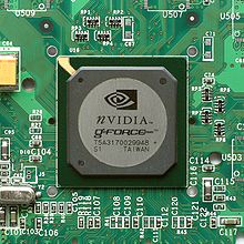
Nvidia GeForce 256 series
The GeForce 256 series , often simply referred to as GeForce , was the first series of graphics processors from the manufacturer Nvidia with the name GeForce and was presented on August 31, 1999. It was the direct successor to the TNT2 and was one of the first series to have a graphics processor with a hardware T&L unit .
Graphics processors
Only one graphics processor is used within the GeForce 256 series, the NV10. Compared to the NV5 chip, which is used in the previous Riva TNT2 series, it offers twice as many rendering pipelines . Together with a smaller manufacturing process, Nvidia was able to achieve a fill rate almost twice as high at TNT2-like clock frequencies. In addition, the NV10 offers the option of being operated with DDR memory , which noticeably increases memory throughput.
The main feature of the GeForce 256 series, however, is the newly added Transform-and-Lighting-Unit (T&L), a kind of specialized, integrated coprocessor that has the purpose of shifting calculations on the object geometry from the CPU to the graphics processor. With previous graphics cards, they only received finished polygon and texture data that only had to be rendered and output. The T&L unit should now take further load off the CPU, as changes to the geometry ( Transform ) and the lighting of the world ( Lighting ) can now be communicated via commands from the graphics card - the CPU ideally saves a lot of time, which increases performance increases. This innovation was implemented hesitantly at first, but it laid the foundation for geometry and exposure calculations using shaders , which found its way into the later generations of graphics cards.
| Graphics chip |
production | Render pipelines | API support | Bus interface stelle |
|||
|---|---|---|---|---|---|---|---|
| production process |
transis- interfere |
The surface |
Pipes × TMU | DirectX | OpenGL | ||
| NV10 | 220 nm | 17 million | 111 mm² | 4 × 4 | 7th | 1.2 | AGP 4x |
Model data
| model | Official launch |
Graphics processor (GPU) | Graphics memory | ||||||
|---|---|---|---|---|---|---|---|---|---|
| Type | Clock rate (MHz) |
Fill rate ( MT / s) |
Size ( MB ) |
Clock rate (MHz) |
Type | Storage interface |
Bandwidth ( GB / s) |
||
| GeForce 256 | Oct 11, 1999 | NV10 | 120 | 480 | 32 64 |
166 | SDR | 128 bit | 2.7 |
| Feb. 1, 2000 | 32 64 |
150 | GDR | 128 bit | 4.8 | ||||
- Note
- The specified clock rates are those recommended or specified by Nvidia. However, the final determination of the clock rates is in the hands of the respective graphics card manufacturer. It is therefore entirely possible that there are or will be graphics card models that have different clock rates.
See also
Individual evidence
- ↑ Nvidia GeForce 256 product page at Nvidia
