
Or gate
| Gate types | |
|---|---|
| NOT | |
| AND | NAND |
| OR | NOR |
| XOR | XNOR |
An OR gate is a gate with several inputs and one output, the output of which delivers a 1 if a 1 is present at at least one input. It corresponds to the logical OR . In switching algebra , the OR link is represented by + or (origin is the Latin word “vel” (or)) and is also referred to as a disjunction .

Overview
| function | Circuit symbol | Truth table | Relay logic | |||||||||||||||||
|---|---|---|---|---|---|---|---|---|---|---|---|---|---|---|---|---|---|---|---|---|
| IEC 60617-12 | US ANSI 91-1984 | DIN 40700 (before 1976) | ||||||||||||||||||
|
|
 |
|
 |
|

|
|||||||||||||||


The greater or equal sign ≥ with the circuit symbol currently valid in Germany shows that if there are one or more ones at the inputs (high, logical 1), the output is 1.
OR gate with a larger number of inputs
The minimum OR gate has two inputs (OR 2 ), but gates with more inputs are also available. If you are limited to gates with a certain number of inputs, you can also use these to implement gates with a higher or lower number of inputs. To increase it, connect several gates, as can be seen in Fig. 1 and 2. In order to reduce the gate runtime and the required number of gates , you should ensure that the structure is as optimal as possible.
If, on the other hand, you need gates with a smaller number of inputs, the inputs that are not required must be connected to logic 0 (often ground, zero potential), see Fig. 3. In Fig. 4, the circuit symbol for an OR gate with three inputs is shown. OR gates with more inputs are drawn accordingly.

Fig. 1: OR 4 gate composed of OR 2 gates in an economical way

Fig. 2: OR 4 gate made of OR 2 gates in an unfavorable way
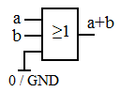
Fig. 3: OR 3 gate reduced to an OR 2 gate
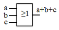
Fig. 4: OR 3 gate


Circuit implementation
OR gates are produced as an integrated circuit (IC) by many manufacturers. Standard modules of this type are z. B. available under the designation "7432" in TTL technology and as "4071" in CMOS technology and contain four OR gates with two inputs each. The exact component designation depends on the manufacturer. Logic gates of this type are available from electronics retailers for a few cents.

Electrical implementation of an OR gate with switches

Realization of an OR gate with relay

In the case of open collectors connected in parallel , one speaks of a " wired OR " ( Wired-OR ), since an OR function is formed here. The signal at the collectors is negative (NOR gate), relative to the pull-up resistor or the component to be controlled, positive.
CMOS

The figure opposite shows the circuit diagram of an OR gate in CMOS technology. The transistors T1 to T4 together form a NOR gate . Is z. B. at input A or B high potential, then conducts T3 or T4, whereby T1 or T2 blocks. At the output of the NOR gate, the transistors T5 and T6 implement the functionality of a NOT gate. A negated NOR gate results in the desired OR gate. With the mentioned input assignment at A and B, there is low potential at T5 and T6 and T5 conducts, but T6 blocks. This results in high potential at output Y.
literature
- Ulrich Tietze, Christoph Schenk: Semiconductor circuit technology . 12th edition. Springer, 2002, ISBN 3-540-42849-6 .