
Wave soldering
Wave soldering or wave soldering is a soldering process with which electronic assemblies ( printed circuit boards , flat assemblies ) are soldered semi- or fully automatically after assembly.

Procedure
Flux application


The soldering side of the circuit board is first wetted with a flux in the fluxer . This can be done by spraying (spray fluxing) or foaming (foam fluxing). Spray fluxers enable finer dosing by defining the mass flow rate. With spray fluxers, the area in which the flux is applied in the x and y directions can be defined using start and end points.
Suction prevents flux vapor from escaping from the fluxer.
Preheating

The circuit board is then preheated using convection heating (swirling the heat, which means that the same temperature is practically everywhere, including on the top), filament heating or infrared radiators . This is done, on the one hand, to evaporate the solvent content of the flux (otherwise blistering during the soldering process), to increase the chemical effect of the activators and to avoid temperature distortion of the assembly and damage to the components due to excessive temperature rise during subsequent soldering. As a rule, a temperature difference of less than 120 ° C is required. This means that at a soldering temperature of 250 ° C, the board must have been warmed up to at least 130 ° C.
Exact data result from temperature profiles. Temperature sensors are attached to relevant points on a sample board and recorded with a measuring device. This gives you temperature curves for the top and bottom of the board as well as selected components.
Soldering process
Now the assembly is driven over one or two solder waves. The solder wave is created by pumping liquid solder through an opening. With the chip wave this is done through a gap, with the Wörthmann wave through the holes of a perforated plate, otherwise the solder wave is created through the elongated holes of a perforated plate.
Double wave systems (chip and delta wave) have been almost completely replaced by the Wörthmann wave (single wave system).
Advantages of a single wave:
- no double temperature load and
- Avoidance of dry soldering of the assembly due to removed flux.
Advantages of the Wörthmann shaft:
- complete wetting of SMD pads,
- few errors in wetting due to shadow effects,
- good soldering of difficult cases ( SOT 23 ) and
- fewer solder bridges with SMD pads.
parameter
The soldering temperature for lead-containing solders is 250 ° C, for lead-free solders 10 to 30 ° C higher, at 260 to 280 ° C.
Background: Especially when a system is mixed with equipment, 260 ° C is used, as there are still a large number of components that, according to the data sheet, can only tolerate 260 ° C. Some customers of the system service provider also require a soldering temperature of a maximum of 260 ° C or only give approval for this. From 260 ° C the alloying also increases disproportionately. The relatively small process window is then a disadvantage .
The soldering time should be chosen so that the heating does not damage the circuit board or the heat-sensitive components. The soldering time is the contact time of the liquid solder per solder joint. The guide times are less than one second for circuit boards laminated on one side and no more than two seconds for circuit boards laminated on both sides. Individual soldering times apply to multi-circuit boards, 2 to 3 seconds for the 3-hole Wörthmann wave and 4 to 6 seconds for the 5-hole Wörthmann wave. According to DIN EN 61760-1: 1998, the maximum time for one or two waves together is 10 seconds.
The immersion depth of the circuit board is to be set so that it is not possible for the shaft to wash over it.
The lead angle is between 5 and 10 °, with 7 ° being the most commonly used (some soldering systems have a non-adjustable soldering angle of 7 °). The inclination of the transport path towards the solder surge depends on the course of the rows of pins on the components. In the case of ladders that run predominantly in the longitudinal direction to the surge - in terms of flow technology - the passage angle should be chosen to be flatter than in the case of predominantly transverse rows of pins. In the case of larger connected copper surfaces (shielding surfaces) on the soldering side, drive flat because otherwise the solder can flow unhindered along the circuit board out of the solder container of the wave soldering system. The setting of the passage angle also determines the solder thickness at the soldered joints. The flatter the lead angle, the more solder remains on the soldered joints. The risk of drops and bridges forming increases. The steeper the draft angle, the more economical the solder deposition.
The shape of the wave depends on the application and is of crucial importance for the end result. Waveforms commonly used today are Chip, Lambda and Wörthmann waves. Usually two waves (chip and delta wave) are used directly one behind the other in order to cope with more complex soldering situations. Thus SMD components on the PCB bottom and wired components are securely soldered on the top side in the same operation on the board (THT). In the case of printed circuit boards with only THT components, only the delta wave is usually required. With the Wörthmann shaft, SMD and THT components can be soldered at the same time.
cooling
After soldering, it makes sense to cool the assembly in order to keep the thermal load within limits. This is done via direct cooling by a cooling unit immediately after the soldering area and / or conventional fans in the lowering station or a cooling tunnel in the return conveyor.
application

Wave soldering is mainly used when soldering circuit boards that are partially or exclusively equipped with THT components. With a larger number of THT components or soldering points, it is usually more economical compared to selective soldering, since it usually takes less time. In the field of power electronics , where very massive or large components often have to be soldered, wave soldering is often the only economically viable soldering technique.
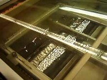
Wave soldering is also important when assembling SMD components on the underside of the circuit board. The individual components must be glued to the circuit board . In the case of components with a narrow pin spacing, such as integrated circuits, in addition to a specific orientation in relation to the direction of the soldering wave, special copper surfaces (pads) are required on the interconnect to avoid short circuits caused by the wave soldering process. To serve z. B. the two spade- shaped soldering surfaces on the left side of the IC shown in the adjacent figure , which strip off the solder of the wave. The direction of the solder wave comes from the right edge of the picture.
In the course of the miniaturization of the assemblies, wave soldering has in many cases been replaced by reflow soldering since the late 2000s , with which SMD components can be assembled more economically. The special soldering areas on the circuit board shown in the illustration are also omitted.
Protective gas
Today wave soldering usually takes place in a protective gas atmosphere. With the use of nitrogen , the negative influence of oxygen on the soldering process is avoided. In practical use, residual oxygen levels of around 100 ppm can be achieved with tunnel systems.
The use of nitrogen offers the possibility of reducing costs and making the process safer. In particular, reworking and repairs to soldered joints can be avoided.
Further advantages of using nitrogen as a process gas are:
- Improved solder connections due to higher wetting speeds
- Significantly reduced solder consumption by reducing tin-lead oxides (dross)
- Reduced flux consumption, mildly activated flux
- Cleanliness of the printed circuit boards
- Reduced maintenance effort
- Environmentally friendly soldering
- Possibility of using lead-free solders
The nitrogen is blown into the soldering area and kept in this area by the precise setting of the suction (at the beginning and end of the machine). Values of 25 to 50 ppm are considered a good residual oxygen content . Below 25 ppm, tin pearls form in the entire soldering area, from 100 ppm (lead-free) slag forms in and around the soldering nozzles, with lead-containing tin only from 200 ppm. So that the soldering quality is not impaired, the slag must be removed at regular intervals when cleaning the system. Without the use of nitrogen, there is an extremely strong formation of slag on the solder container.
Variations
Selective soldering


A variant of wave soldering that is becoming more and more important is selective wave soldering. In this case, not the entire assembly, but only a small part of it is soldered using a "miniature wave". The effectively soldered area can be only a few square millimeters, depending on the shape of the soldering nozzle. The assembly is brought exactly over the shaft with a positioning device. To do this, each component to be soldered must be entered into the soldering program with the exact values of the x and y axes (e.g. for a pin header with 10 pins, the start coordinate of the first pin and the end coordinate of the last pin). The clamp frame or the inlay with the assembly (s) is first moved over the preheating field and heated. The flux is usually applied through one or two very small spray nozzles, only the pins / rows of pins to be soldered are sprayed. Soldering works the same way as fluxing, pin by pin for each component. Individual pins through individual approach, called point soldering. Several pins (plugs, pin headers) by lowering them to the first pins and driving a track until shortly after the last pin. If only one assembly fits into the frame, a fluxer and soldering nozzle is used. If two or a multiple of two fit into the frame, two fluxer and soldering nozzles can be used. In selective soldering systems it is also easily possible to use a crucible with lead-free tin in addition to one crucible with lead-free tin. When changing a product between the crucibles, only the offset or the position of the second crucible needs to be entered in the soldering program. Selective soldering is used when many SMD components have already been soldered on a circuit board in a reflow process and only a few THT components need to be soldered. A second thermal stress for the circuit board and the components on it can thus be avoided. Another area of application is the soldering of components on the soldering side, after wave soldering.
Selective soldering using the stroke / immersion method is a variant in which a product-specific multiple nozzle soldering tool is used, then all components provided for this are soldered at the same time by lowering the circuit board onto the arranged nozzles. Several miniature waves form a multiple wave system here.
The selective soldering process is often the only possible soldering process when components that are wired on both sides have to be soldered and wave soldering with the classic wave is no longer possible on the second side of the assembly. Compared to a classic wave soldering system, the selective soldering system usually takes up significantly less space. The selective soldering technology is particularly economical when a few components or a few individual pins have to be soldered.
Repair soldering
Repair soldering systems have a miniature wave (depending on the type of wave shaper from 10 cm × 3 cm to 25 cm × 10 cm). If, after wave soldering, it is found that components are not resting on the circuit board or have been soldered upside down, rework must be carried out. Typical applications here are components with many pins (plugs, pin strips, ...) or components that have a high heat absorption capacity and cannot be replaced with other repair soldering processes, or only with considerable effort. During repair soldering, flux is applied to the affected area of the assembly and the assembly is placed in the liquid solder of the surge bath. The heat input of the liquid solder melts the solder of the components on the circuit board so that the component concerned can either be aligned or pulled out. When a component is replaced, a new component is immediately placed in the circuit board. The liquid solder creates the soldered connection between the component and the circuit board.
literature
- Reinard J. Klein Wassink: Soft soldering in electronics . 2nd Edition. Eugen G. Leuze, Saulgau 1991, ISBN 3-87480-066-0 .
- Wolfgang Scheel (Hrsg.): Assembly technology of electronics . Verlag Technik u. a., Berlin a. a. 1997, ISBN 3-341-01100-5 .