
Extended Data Output Random Access Memory

The EDO RAM ( E xtended D ata O utput RAM , also known as Hyper Page Mode RAM hereinafter) is a semiconductor memory . It belongs to the group of DRAMs . It represents a slight development of the FPM RAM ( F ast P age M ode RAM ). Due to its elevated data transfer rate began this starting around 1996 to replace.
Details
The difference between EDO and FPM RAM is only noticeable in the so-called pagemode mode, in which several data bits are read from the same memory page ( page ). In this case all have the same row address ( Row Address ), but different column addresses ( column address ). The protocol can be simplified - both with the FPM-RAM and the EDO-RAM - by omitting the transmission of the unchanged line address. To read out data from the memory page, only the transmission of the column address is necessary.
The validity of the column address is indicated by a falling edge (see diagram for read access ) at the external CAS control input ( Column Address Strobe ). After a certain delay, the DRAM makes the new data available at its outputs. The EDO-RAM differs from the FPM-RAM in one small detail. Although the FPM and EDO-RAM memory modules intended for computer main boards (“mainboards”) physically fit into the same slots, EDO-RAM either does not work in mainboards without EDO support or is addressed like FPM. Conversely, however, mainboards with EDO support can almost always be operated with FPM-RAM. EDO-RAM is available with access times of 70 ns, 60 ns and 50 ns. EDO-RAM with 70 ns access time can cause problems on mainboards that operate the front side bus at 66 MHz. The versions with a maximum capacity of 32 MiB have found the most widespread use, whereas those versions with a capacity of 64 MiB or more have often proven to be incompatible with the mainboards available on the market. Later there were even modules with 128 MiB, but because of the dominance of SDRAM at the time, they were no longer sold in large numbers.
In the older FPM-RAM, the invalidation of the column address is signaled by the rising edge of the CAS control line. As a result, the FPM-RAM deactivates its data drivers, whereby the previously valid date disappears from the external data outputs (see diagram for page mode ). The status of the data outputs remains undefined until the process is repeated by specifying a new column address and a falling edge on the CAS line. The FPM-RAM makes the data read out in the pagemode available at its outputs for only a fraction of the cycle time .
With the newer EDO-RAM, however, the rising edge of the CAS control line is ignored. The data drivers remain active and the previously read data information remains at the external data outputs until it is replaced by new information (see diagram for EDO mode ).
This modification of the protocol does not initially result in any increase in the data transfer rate. All that is achieved is that the data read out is available at the external data outputs during the entire pagemode cycle time. The extended availability time of the read-out data with EDO-RAM made it possible to better utilize the increase in speed associated with the further development of DRAMs by further reducing the cycle time in pagemode . The extended availability time of the data within a cycle ensured that the data could be read out reliably despite the reduced cycle time. The performance gain of the EDO-RAM achieved in Pagemode was usually overestimated and was only in the range of a few percent.
Later developments
With the BEDO-DRAM , the internal control of the EDO-RAM has been modified so that the data of several consecutive memory addresses can be read out together in a single clock cycle. This technology could not establish itself on the market.
EDO-RAM has been replaced by SDRAM in almost all areas of application .
Diagrams of selected commands (simplified representation)
Read and write access

Read access ("Read")
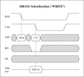
Write access ("Write")


Read access in page mode and hyper page mode (EDO)
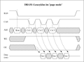
Read access in "page mode"
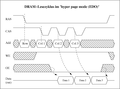
Read access in "hyper page mode" (EDO)


Refresh modes
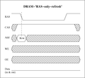
RAS-only -refresh
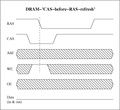
CAS-before-RAS -refresh ("CBR refresh")

hidden -refresh in the read cycle

self -refresh


literature
- SIEMENS Memory Components Data Book 10.96, Ordering No. B 166-H6557-G3-X-7600