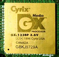
Cyrix MediaGX
| MediaGX, MediaGXi, MediaGXm | |
|---|---|
 Cyrix MediaGX 133 MHz processor |
|
| Production: | 1997 to 1998 |
| Producer: | Cyrix , IBM |
| Processor clock: | 120 MHz to 300 MHz |
| FSB cycle: | 33 MHz to 66 MHz |
| L1 cache size: | 16 KiB |
| Instruction set : | x86 |
| Base: | based on socket 7 |
The Cyrix MediaGX CPUs were the first x86 CPU that emerged as a SoC design. The Cyrix 5x86 processor was used as the basis and additional functions of the Northbridge and other system components such as B. a memory controller and a graphics chip integrated into the processor.
National Semiconductor , the parent company of Cyrix, concentrated heavily on these SoC chips and so the division was not sold even after Cyrix was bought on to VIA Technologies , but development was continued under the new name Geode . The MediaGX is thus the basis for the current Geode SoCs.
Model data
MediaGX GX
- L1 cache: 16 KiB (unified)
- Socket with 352 pins, based on socket 7
- Front Side Bus : 33 MHz
- Operating voltage (VCore): 3.3, 3.6 V.
- Power consumption ( TDP ):
- Release DATE: 1997
- Manufacturing technology: 0.4 µm at IBM
- The size: 160 mm² with 2.4 million transistors
- Clock rates: 120, 133 and 150 MHz
- Housing: BGA -352 (plastic, metal)
MediaGX GXI
- L1 cache: 16 KiB (unified)
- Socket with 352 pins, based on socket 7
- Front Side Bus : 60 and 66 MHz
- Operating voltage (VCore): 2.9V
- Power consumption ( TDP ):
- Release DATE: 1997
- Manufacturing technology: 0.35 µm at IBM
- The size: 160 mm² with 2.4 million transistors
- Clock rates: 120, 133, 150, 166 and 180 MHz
- Housing: BGA-352 (plastic, metal)
MediaGX GXm
- L1 cache: 16 KiB (unified)
- MMX
- Socket with 352 pins, based on socket 7
- Front Side Bus : 60 and 66 MHz
- Operating voltage (VCore): 2.2, 2.5, 2.9 V.
- Power consumption ( TDP ): max. 11.27 W (at 300 MHz)
- Release DATE: 1998
- Manufacturing technology: 0.35 µm at IBM
- The size: 160 mm² with 2.4 million transistors
- Clock rates: 180, 200, 233, 266 and 300 MHz
- Housing: BGA-352 (plastic, metal), PGA -296 (ceramic)
MXi
- Code name: Cayenne (for the CPU)
- L1 cache: 64 KiB (unified)
- MMX , 3DNow
- based on the base 370
- Front Side Bus : 100 MHz
- Operating voltage (VCore):
- Power consumption ( TDP ):
- Publication date: never published
- Manufacturing technology: 0.25 µm
- Clock rates: approx. 300 MHz
Web links
- GXM CPUs ( Memento October 12, 2007 on the Internet Archive ) - National Semiconductor Product Page
- AMD Geode Family - Official Product Page
- Cyrix MediaGX and National Semiconductor Geode Information - cpushack.net
- Cyrix Media GX CPU
Individual evidence
- ↑ Cyrix MediaGX ( English ) pctechguide.com. April 11, 2006. Retrieved January 6, 2011.


