AMD Geode
| Geode | |
|---|---|
 |
|
| Production: | since 2000 |
| Producers: | |
| Processor clock: | 200 MHz to 1.4 GHz |
| FSB cycle: | 66 MHz to 266 MHz |
| L2 cache size: | 0 kB to 256 kB |
| Instruction set : | x86 |
| Microarchitecture : | Cyrix / AMD K7 |
Base:
|
|
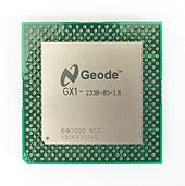
The SoC family of Geode processors has been specially developed for the embedded and low-power sector. The geode has a very eventful history and was originally developed by Cyrix under the name Cyrix MediaGX . With the acquisition of Cyrix, this know-how passed to National Semiconductor . These concentrated heavily on these SoC circuits, so the division was not sold even after Cyrix was bought on by VIA Technologies , but development continued under the new name Geode . The result was the National Geode GX1 and GX2.
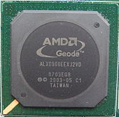
For economic reasons, National sold the corresponding SoC division to AMD in 2003 . Since then, these processors have been developed and produced by AMD until AMD integrated Geode development into the 64-bit development department in July 2006. However, AMD had already licensed the technology to the Chinese Ministry of Science and Technology (MOST) and Beijing University on October 24, 2005.
AMD Fusion can now be seen as the successor to AMD Geode . These so-called APUs are a combination of economical x86 main processors with an integrated graphics processor , which were specially developed for very economical and attractively priced systems.
National Semiconductor
Geode GX1
After National Semiconductor took over Cyrix , the National Geode GX1 was developed based on the old Cyrix MediaGX . Among other things, the memory interface of the memory controller that is also integrated has been made suitable for SDRAM.
Geode GX2
The National Geode GX2 is the fundamentally revised successor to the Geode GX1 and is u. a. equipped with a larger L1 cache, AMD's 3DNow instructions and a longer pipeline . The FPU has also been improved (is now fully pipelined ), and the memory interface of the memory controller, which is also integrated, has been changed to DDR-SDRAM .
Model data
Geode GX1
- L1 cache: 16 kB (unified)
- MMX
- GeodeLink Interface (based on Socket 7 )
- Front Side Bus : NA
- Storage cycle: max. 111 MHz
- Operating voltage (VCore): 1.6 V to 2.2 V.
- Power consumption ( TDP ): max. 1.4W @ 2.2V / 333 MHz
- Release DATE: April 12, 2000
- Manufacturing technology: 0.18 µm
- Clock rates: 200, 233, 266, 300 and 333 MHz
Geode GX2
- L1 cache: 16 + 16 kB (data + instructions)
- MMX , 3DNow
- GeodeLink Interface (based on Socket 7 )
- Front Side Bus :
- Operating voltage (VCore):
- Power consumption ( TDP ):
- Release DATE: October 17, 2001
- Manufacturing technology: 0.15 µm at National
- Clock rates: 266, 333 and 400 MHz
- The processor has been discontinued for 2009 and there is no direct successor
Geode GXLV
- L1 cache: 16 kB (unified)
- MMX
- Front Side Bus :
- Operating voltage (VCore): 2.2V, 2.5V, 2.9V
- Operating voltage (I / O): 3.3V (5V tolerant)
- Power consumption (typical): 1.0W at 2.2V / 166 MHz and 2.5W at 2.9V / 266 MHz
- Publication date:
- Manufacturing technology: 0.25 µm four layer CMOS
- Clock rates: 166, 200, 233, 266 MHz
- Housing: 352-pin terminal BGA or 320-pin SPGA
Advanced Micro Devices
Geode GX
The AMD Geode GX has the same specifications as the National Geode GX2. In order to upgrade the already aged design, AMD decided to introduce a P rating to ensure comparability with the competition (especially VIA C3 ). AMD's P-Rating of the AMD Geode GX is reminiscent of the old P-Rating from Cyrix, which was never really true: Comparative tests have shown that AMD's Geode GX remains below the performance of its competitors. However, it is positive that AMD also adds the power consumption to the P rating. However, the average consumption is given, not the TDP , which means that under high loads the power loss is significantly higher than the P-rating suggests. AMD guaranteed availability until December 31, 2009.
Geode LX
The AMD Geode LX is the further development of the AMD Geode GX and is therefore also very much based on the processor architecture from National or Cyrix . However, AMD has made changes to this CPU: The L1 cache was enlarged to 128 kB and an L2 cache with 128 kB was added. It was also an already from Centaur Nehemiah known AES integrated storage engine. This made the CPU more powerful than its predecessor, but its P-rating and the stated consumption are very dubious. These changes attempt to make the outdated CPU design more competitive. A 600 MHz version was announced in February 2007. AMD plans the availability of the processor family until 2015. According to AMD's embedded roadmap, the Geode LX CPU will be improved in detail in the future.
Geode NX

With the Geode NX, AMD is trying for the first time to advance on a larger scale into a market segment that primarily dominates VIA Technologies with EPIA boards (based on CPUs from Centaur Technology ). In further cooperation with SiS , LogicPD developed a mini-ITX board that is very reminiscent of VIA's EPIA series in terms of equipment.
Contrary to what the name suggests, the Geode NX is not a further development of the original Geode design, but a processor based on the Athlon XP. Both processor families are sold in parallel by AMD and fundamentally differ in their architecture. The Geode NX is a low-clocked and low-voltage Thoroughbred B, which has already been used in the Athlon XP , Athlon MP and, last but not least, in the Athlon XP-M and is now once again being honored. The support provided by chipsets and software is correspondingly good, of course, which is definitely an advantage for AMD. As usual with AMD since the Athlon XP, the Geode NX also has model numbers to classify the performance.
Geode NX 2001
In 2007, a Geode NX 2001 was sold that was a renamed Athlon XP 2200+ Thoroughbred. The processors with part numbers AANXA2001FKC3G or ANXA2001FKC3D had a clock frequency of 1.8 GHz and a core voltage of 1.65 volts, but the power consumption was not specified. There are no official declarations for this processor , only a few copies have been shipped to special customers. Nevertheless, apart from the same CPU socket ( socket A ), it doesn't seem to have any connection with the other Geode NX processors.
Model data
Geode GX
- L1 cache: 16 + 16 kB (data + instructions)
- MMX , 3DNow
- GeodeLink Interface (based on Socket 7 )
- Clock rates: 333 MHz to 400 MHz
- [email protected]: 333 MHz
- [email protected]: 366 MHz
- [email protected]: 400 MHz
Geode LX
- Code name: Castle
- L1 cache: 64 + 64 kB (data + instructions)
- L2 cache: 128 kB with processor clock
- MMX , 3DNow
- GeodeLink Interface (based on Socket 7 )
- Release DATE: May 2005
- Manufacturing technology: 0.13 µm at TSMC
| Model name | Clock rate MHz | Supply voltage | TDP in watts | Ambient temperature range | Storage type |
|---|---|---|---|---|---|
| [email protected] | 600 | 1.4V | 5.1 | 0˚C to 80˚C | DDR-400 |
| [email protected] | 500 | 1.25V | 3.6 | 0˚C to 85˚C | DDR-400 |
| [email protected] | 500 | 1.25V | 3.6 | -40˚C to 85˚C | DDR-400 |
| [email protected] | 433 | 1.2V | 3.1 | 0˚C to 85˚C | DDR 333 |
| [email protected] | 366 | 1.2V | 2.8 | 0˚C to 85˚C | DDR-266 |
Geode NX
- Code name: Thoroughbred B
- L1 cache: 64 + 64 kB (data + instructions)
- L2 cache: 256 kB with processor clock
- MMX , Extended 3DNow , SSE , PowerNow!
- Socket A , EV6 with 133 MHz (FSB 266)
- Operating voltage (VCore):
- 1250 @ 6W: 1.1V
- 1500 @ 6W: 1.0V
- 1750 @ 14W: 1.25V
- Power consumption ( TDP ):
- 1250 @ 6W: 9 W max.
- 1500 @ 6W: 18 W max.
- 1750 @ 14W: 25 W max.
- First release date:
- Manufacturing technology: 0.13 µm
- Clock rates: 667 MHz to 1,400 MHz
- 1250 @ 6W: 667 MHz
- 1500 @ 6W: 1,000 MHz
- 1750 @ 14W: 1,400 MHz


