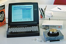
Scanning probe microscopy


Scanning probe microscopy ( english scanning probe microscopy SPM) is the umbrella term for all types of microscopy in which the image is not with an optical or electron-optical imaging ( lenses produced) as the light microscope (LM) or scanning electron microscope (SEM), but about the Interaction of a so-called probe with the sample. The sample surface to be examined is scanned point by point using this probe in a raster process. The measured values resulting for each individual point are then combined to form a digital image.
functionality
Roughly simplified, one can imagine how an SPM works like scanning a record with the needle. However, with the turntable the needle is deflected purely mechanically by microscopic unevenness in the groove. With SPM, however, the interaction between the probe (needle) and the sample is of a different nature. Depending on the type of interaction, a distinction is made between the following types of SPM:
- Scanning tunnel microscope (RTM), engl. scanning tunneling microscope (STM): A voltage is applied between the sample and tip, which do not touch each other, and the resulting tunneling current is measured.
- Atomic Force Microscope (RKM), engl. atomic force microscope (AFM, also SFM): The probe is deflected by atomic forces, typically van der Waals forces . The deflection is proportional to the force, which can be calculated using the spring constant of the probe.
- Magnetic force microscope (MKM), engl. magnetic force microscope (MFM): The magnetic forces between the probe and the sample are measured here.
- Optical scanning near field microscope , engl. near-field scanning optical microscope (SNOM, also NSOM): The interaction here consists of evanescent waves .
- Acoustic scanning near field microscope , engl. scanning near-field acoustic microscope (SNAM or NSAM)
The following size comparison is interesting: If the atoms in the sample were the size of table tennis balls, the probe (measuring tip) would be the size of the Matterhorn . The fact that one can scan such fine structures with such a coarse tip can be explained as follows. Atomically speaking, however blunt the tip of the probe may be, some of the atoms will be on top. Since the interactions between sample and tip decreases exponentially with the distance between sample and tip, only the foremost (topmost) atom of the tip makes a significant contribution.
Resolving power and single atom manipulations
With this method, resolutions of up to 10 picometers (pm) can be achieved ( atoms have a size in the range of 100 pm). Light microscopes are limited by the wavelength of the light and usually only achieve resolutions of approx. 200 to 300 nm, i.e. about half the wavelength of light. In the scanning electron microscope, therefore, electron beams are used instead of light. Theoretically, the wavelength can be made as small as desired by increasing the energy, but the beam then becomes so “hard” that it would destroy the sample.
SPM can not only scan surfaces, but it is also possible to remove individual atoms from the sample and place them back at a defined location. Such nanomanipulations became known through the image of the IBM research laboratory, on which the company's lettering was represented by individual xenon atoms.
With a variant of the atomic force microscope by Leo Gross and Gerhard Meyer , the usability for the chemical structure elucidation of, for example, organic molecules was demonstrated in 2009 and Michael Crommie and Felix R. Fischer followed a reaction of aromatics in organic chemistry in 2013.
Influence on the natural sciences
The development of scanning probe microscopes since the beginning of the 1980s was an essential prerequisite for the explosive development of nanosciences and nanotechnology since the mid-1990s due to the significantly improved resolution of well below 1 μm and the possibility of nanomanipulation . Starting from the basic methods described above, a distinction is made today between many other sub-methods that address certain additional aspects of the interaction used and are reflected in a variety of extended abbreviations:
- STS ( scanning tunneling spectroscopy ),
- STL ( scanning tunneling luminescence ),
- XSTM ( cross-sectional scanning tunneling microscopy ),
- XSTS ( cross-sectional scanning tunneling spectroscopy ),
- SPSTM ( spin-polarized scanning tunneling microscopy ),
- VT-STM ( variable temperature scanning tunneling microscopy ),
- UHV-AFM ( ultrahigh vacuum atomic force microscope ),
- ASNOM ( apertureless scanning near-field optical microscopy ) and much more
Analogously, research areas such as nanobiology , nanochemistry , nanobiochemistry, nanotribology, nanomedicine and many more emerged. An AFM ( atomic force microscope ) has even been sent to the planet Mars to examine its surface.
See also
- Gerd Binnig , physicist, Nobel Prize winner and inventor of the STM
- Nanomanipulator
literature
- B. Voigtländer: Scanning Probe Microscopy . Springer, 2015, ISBN 978-3-662-45239-4 , doi : 10.1007 / 978-3-662-45240-0 .
- B. Voigtländer: Atomic Force Microscopy . Springer, 2019, ISBN 978-3-03013653-6 , doi : 10.1007 / 978-3-030-13654-3 .
- C. Julian Chen: Introduction to Scanning Tunneling Microscopy . Oxford University Press, Oxford 1993, ISBN 0-19-507150-6 (English).
- Roland Wiesendanger : Scanning Probe Microscopy and Spectroscopy - Methods and Applications . Cambridge University Press, Cambridge 1994, ISBN 0-521-42847-5 (English).
Individual evidence
- ↑ IBM lettering made of individual xenon atoms
- ↑ First AFM on Mars , contains animations on how the AFM works