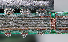
Ball Grid Array

Ball Grid Array ( BGA , engl.) To German ball grid array is a housing shape of integrated circuits , in which the connections for SMD -Bestückung lying compactly on the underside of the component.
The terminals are small solder balls (engl. Balls ) arranged side by side (engl. In a raster grid ) are made up of columns and rows. During reflow soldering, these beads are melted in a soldering oven and connect to the contact pads on the circuit board .
This design represents a solution to the problem of accommodating a very large number of connections on one component. In contrast to dual in-line designs, the pins can be arranged in several rows and their number can be multiplied. Compared to pin grid arrays , BGAs allow a connection density that is about twice as high.
The chips can, despite the flat soldering, for. B. be removed (unsoldered) from the circuit board with hot air without being damaged. The chips are then optionally from old solder balls freed (entlotet, Eng. Deballing ), cleaned and stocked with new solder balls (Neubeperlung, Eng. Reballing ). They can then be soldered back onto a new circuit board. This technique can also be used to replace defective chips when repairing circuit boards. However, compared to conventional designs, it requires great skill and suitable tools.
advantages
The advantages of the BGAs are in the area of only a very small space requirement, the good heat dissipation of the resulting power loss in the component towards the circuit board and the low impedance due to short connections to the circuit board. Furthermore, BGA structures are self-centering during reflow soldering when the maximum displacement between ball and pad is less than 50% of the structure width. In this case the BGA centers itself through the surface tension of the solder . Furthermore, BGAs have the advantage that manipulation of safety-relevant circuits and imitation are made more difficult due to the special soldering technology required.
disadvantage
In addition to the advantages described above, BGAs have decisive disadvantages that must be particularly taken into account when using this form of housing. This includes, for example, the inspection and repair of soldered joints. In addition to X-ray and ultrasound methods, direct visual inspection is only possible to a limited extent. In addition, mechanical stresses in the circuit board are transferred to the component more strongly than with wired components or with components with gull -wing connections of the pins. Furthermore, these components can only be securely soldered with special equipment (regulated soldering furnace). In addition, commissioning, measurements and repairs are made much more difficult because the connections are more difficult to access.
Many modern semiconductors are only manufactured in BGA housings, and BGAs are very difficult or even impossible to process for hobby electronics . B. a reflow oven required. In addition, BGAs can only be used sensibly on multilayer boards . However, multilayer circuit boards are very expensive if they can be produced as a single piece or in small series by a circuit board manufacturer through inexpensive suppliers in Asia, but multilayer circuit boards are becoming increasingly affordable, which makes them interesting for hobbyists too. As a stopgap solution, hobby electronics engineers can stick the BGA upside down on the circuit board and contact the connections with thin enamelled copper wires. However, this looks very unprofessional and is electrically and especially mechanically not optimal.
Types
Examples of different BGA types:
- BGA - grid 0.7 mm - 2.5 mm
- FBGA - Fine BGA , also Fine Pitch BGA ( JEDEC standard) and Fine Line BGA from the manufacturer Altera , BGA package with reduced solder point distance (0.5 mm - 0.7 mm)
- MBGA - Micro Fine Line BGA 0.5 mm grid
- VFBGA - Very Fine BGA , pitch <0.5 mm
- FCBGA - Flip Chip BGA
- CBGA - Ceramic Ball Grid Array , like BGA in a ceramic housing
- CSP - Chip Scale Package , no BGA belongs to the LLPs ( Lead Less Chip Carrier )
- LFBGA - Low-profile Fine-pitch Ball Grid Array
- PoP - Package-on-Package . Two ball grid arrays are fitted on top of each other.
Testing of BGAs
Detachable adapters, sockets or, for example, rigid needle adapters (contacting pad structures down to a pitch of 150 µm) are required to test BGA circuits .
Related designs
Individual evidence
- ↑ Design Requirements - Fine Pitch Ball Grid Array Package (FBGA) DR-4.27D March 2017, accessed August 16, 2017
- ↑ Board Design Guidelines for Intel Programmable DevicePackages. Retrieved January 18, 2020 .
Web links
- The Ball Grid Array (English; PDF file; 6.53 MB)
- Multi CB PCBs: BGA design suggestions


