Transmission gate
In electronics , especially in microelectronics , a mostly integrated electronic circuit is referred to as transmission gates , transmission gates or transmission gates , which, similar to a relay , can conduct or block continuous currents with almost any voltage potential in both directions using a control signal .
construction
In principle, a transmission gate consists of two field effect transistors in which - in contrast to conventional discrete field effect transistors - the substrate connection (bulk) is not internally connected to the source connection. The two transistors, an n-channel MOSFET and a p-channel MOSFET, are connected in parallel , but only the drain and source connections of the two transistors are connected to one another. In the case of a transmission gate, the gate connections are connected to one another via a non-gate (inverter), whereby a resulting control connection is formed.
If, as is usual with discrete transistors, the substrate connection is connected to the source connection, a diode (substrate diode ) parallel to the transistor results , whereby the transistor always conducts backwards. However, since a transmission gate must be able to block currents in both directions, the substrate connections are connected to the respective supply voltage potential in order to ensure that the substrate diodes are always operated in the blocking direction . The substrate connection of the n-channel MOSFET is accordingly connected to the negative supply voltage potential and the substrate connection of the p-channel MOSFET is connected to the positive supply voltage potential.
function

If a logic zero (negative supply voltage potential) is applied to the control input, the gate connection of the n-channel MOSFET is also at negative supply voltage potential. Due to the inverter, the gate connection of the p-channel MOSFET is at the positive supply voltage potential. Regardless of which switching connection of the transmission gate (A or B) there is a voltage (in the permissible range), the gate-source voltage of the n-channel MOSFET is always negative, that of the p-channel MOSFET always positive be. Accordingly, neither of the two transistors will conduct and the transmission gate blocks.
If a logic one is present at the control input , the gate connection of the n-channel MOSFET is also at positive supply voltage potential. Due to the inverter, the gate connection of the p-channel MOSFET is now at negative supply voltage potential. Since the substrate connection of the transistors is not connected to the source connection, the drain and source connections are almost equivalent, and the transistors begin to conduct when there is a voltage difference between the gate connection and one of these two channel connections.
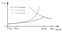
If a voltage in the vicinity of the negative supply voltage potential is now applied to one of the switching connections of the transmission gate, a positive gate-source voltage (gate-drain voltage) occurs on the n-channel MOSFET and the transistor begins to conduct : The transmission gate is conducting. If the voltage at one of the switching connections of the transmission gate is now continuously increased up to the level of the positive supply voltage potential, the gate-source voltage (gate-drain voltage) of the n-channel MOSFET is reduced and the MOSFET begins to block. At the same time, however, a negative gate-source voltage (gate-drain voltage) builds up on the p-channel MOSFET, as a result of which this transistor begins to conduct and the transmission gate continues to switch through.
This ensures that the transmission gate conducts over the entire permissible voltage range. The transition resistance of the transmission gate varies, depending on the voltage to be switched, and corresponds to a superposition of the resistance curves of the two transistors.
application
Electronic switch
Transmission gates are used to implement electronic switches and analog multiplexers . If a signal is to be switched to different outputs ( toggle switch , multiplexer), several transmission gates are used, since a transmission gate can only conduct or not conduct ( simple switch ). A typical representative is the 4-way analog switch known as 4066 , which is available from various manufacturers.
Logic circuits
With the help of transmission gates, logic circuits can be set up. This usually saves transistors and thus space on the silicon compared to conventional logic circuits .
Negative tensions
In order to be able to switch alternating voltages (e.g. audio signal ) with a transmission gate , the negative supply voltage potential must have a potential below the smallest possible signal potential. This ensures that the substrate diodes remain blocked even in the event of negative voltages. In order to still be able to switch the transmission gate with classic logic levels , there are special versions with an integrated level converter .
See also
literature
- Ulrich Tietze, Christoph Schenk: Semiconductor circuit technology. 12th edition, Springer, Berlin / Heidelberg / New York 2002, ISBN 3-540-42849-6 .
- Erwin Böhmer: Elements of applied electronics. 15th edition, Vieweg & Sohn Verlag | GWV Fachverlage GmbH, Wiesbaden 2007, ISBN 978-3-8348-0124-1 .
- Klaus Fricke: Digital technology. 6th edition, Vieweg & Sohn Verlag | GWV Fachverlage GmbH, Wiesbaden 2009, ISBN 978-3-8348-0459-4 .
