TRIPS processor
The TRIPS processor ( T era-op, R eliable, I ntelligently adaptive P rocessing S ystem ) is a research processor of the University of Texas at Austin . The processor architecture is designed in such a way that further cores can be added as easily as possible. The project is funded by IBM and DARPA .
The TRIPS architecture is intended to be a successor to the common RISC architecture and is referred to as the EDGE architecture. The EDGE architecture has blocks that execute elementary instructions independently of one another, as well as data-driven (out-of-order) instruction execution.
TRIPS is being developed to implement processors with more than one teraflop. Even Intel's Intel Tera-Scale is developed in this context, however, is based on a different architecture with similar computing elements.
Structure of the architecture
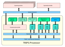
The TRIPS processor consists of one or more arithmetic and logic units (ALU), caches and registers . The ALUs perform integer and floating point arithmetic operations. Separate caches are provided for data and instructions . In addition, several translation buffers (TLB) are provided, which map virtual to physical addresses.
When it comes to registers, a distinction is made between general and special registers ( Special Function Register , SFC ) in TRIPS . General registers are used to store any data or addresses. Special registers are responsible for the configuration and control of the processor status.
In contrast to conventional RISC processors, the TRIPS processor defines a number of internal queues and are part of the instruction set and the data flow model . This enables a series of instructions to be executed as a block instead of just individual instructions. The instruction queue ( instruction queue , IQ ) can this process up to 128 instructions simultaneously, the read queue ( Read queue , RQ ) buffers 32 read accesses to general registers and the write queue ( Write queue , WQ ) buffers up to 32 write accesses to general registers. An additional load and store queue ( LSQ ) buffers 32 memory accesses. Queues only buffer transient states, while persistent states are kept in registers, caches and the system memory.
The rest of the TRIPS consists of a system-wide network that connects the individual calculation blocks with one another. Access by processors that want to access a shared memory via this network is controlled by a system controller.
implementation
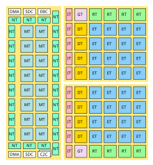
TRIPS processors of individual tiles ( tiles constructed), each tile meets an elementary function. The individual tiles are brought into a two-dimensional arrangement ( array ). A distinction is made between the following types of tiles:
- the Execution Tiles (ET) contain IQ and ALU.
- the Tiles (RT) registers contain general registers, RQ and WQ.
- the data tiles (DT) contain data cache, data TLB and LSQ.
- the instruction tiles (IT) contain instruction cache and instruction TLB.
- the Global Control Tile (GT) contains the special registers and the logic of the global processor controller.
Most of the processor resources are also divided into banks and can therefore be distributed over several tiles. The TRIPS architecture thus forms a grid architecture at the processor level. This allows high clock frequencies , high parallelism of the instructions and good expandability. Since high latencies can occur in such a grid architecture when data has to be brought from a tile to a distant tile, scaling problems could arise, which is why the scalability of the system is currently being investigated in more detail using prototypes.
One advantage of the architecture is that the queues and registers are available multiple times due to the multiple execution of identical tiles. This means that a very large number of instructions and up to four threads can be processed in parallel and thus simultaneously.
First prototype
In the first - in the spring of 2007 realized - TRIPS prototype, two TRIPS processor cores and L2 cache ( Secondary Memory System ) with interfaces to the periphery of the main board on the processor The manufactured.
| Abbreviation | Surname | description |
|---|---|---|
| NT | Network tile | Form a network in which data is transported to and from the memory. |
| MT | Memory tile | Form the memory of the L2 cache in which data is stored. |
| DMA | Direct memory access | Direct memory access controller ( Northbridge ) |
| SDC | Static DRAM controller | Provides memory access to the SDRAM banks of the main memory |
| EBC | External bus controller | Establishes the connection with buses ( South Bridge ) here, which are located outside of the processor, and handles interrupt requests ( interrupt request , IRQ ) and external bus interfaces ( External Bus Interface , EBI ). |
| C2C | Chip-to-Chip Connector | Used to establish a direct connection with other TRIPS processors. The C2C is available four times in the TRIPS processor in order to form arrays from TRIPS processors and thus to be able to build computing clusters . |
The prototype was manufactured as an ASIC in a 130 nm process and consists of around 170 million transistors. The TRIPS processor masters 4-fold multithreading and can execute up to 16 instructions per clock and processor at a clock frequency of 500 MHz. This results in a peak performance of 16 GOps (16 billion operations per second).
Microbuses
The individual tiles in the array are connected to one another via simple micro-networks. A distinction is made between the microbuses listed in the following table:
| Abbreviation | Name of the bus | |
|---|---|---|
| ∎∎∎ | GDN | Global Dispatch Network |
| ∎∎∎ | GSN | Global Status Network |
| ∎∎∎ | OPN | Operand Network |
| ∎∎∎ | GCN | Global Control Network |
| ∎∎∎ | OCN | On chip network |
| ∎∎∎ | GRN | Global Refill Network |
| ∎∎∎ | ESN | External Store Network |
| ∎∎∎ | DSN | Data Status Network |
The colors listed in the table correspond to the colors of the buses in the adjacent illustration.
Execution tile
Each of the 16 Execution Tiles consisting of a simple data pipeline , a bank of 64 reservation stations ( reservation station ) and an integer - as well as a floating point unit. With the exception of the division unit, all units are designed as a pipeline architecture . The division unit requires 24 cycles.
The reservation stations each contain eight instructions for each of the eight TRIPS blocks, which means that the TRIPS blocks are controlled continuously. Each reservation station has fields for two 64-bit operands and a 1-bit predicate .
Tile tab
The TRIPS processor's micro-architecture is divided into registers and banks to reduce power consumption and time delays. Each Tile tab contains a bank and a connection to the operand network. This allows the compiler to place important read / write instructions in a register that is close to the register to be written to or read out.
Which are read immediately after the definition data are not stored by the compiler in the register, whereby the data throughput - bandwidth of the register can be lower by about 70% than in a register of a RISC or CISC processor. The four distributed banks therefore have sufficient bandwidth despite a small number of connections (2 × read and 1 × write).
Each of the four register tiles contains a 32-register bank for each of the four SMT threads supported by the core . In this way, 128 registers are available for each thread, which are distributed over the 128 register banks of the register tiles.
In addition, each register Tile contains a write and a read queue. The write queue contains up to eight read accesses and the read queue contains up to eight write accesses. The queues ensure dynamic and continuous forwarding of access to the registers.
Data tile
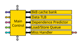
Each data tile is a participant in the operand network. It contains a 2-way L1 cache bank with a size of 8 kB. Virtual addresses are distributed over the data tiles in an interleaving process in a cache row with 64 bytes.
In addition to the L1 cache bank each Data contains Tile a copy of the load / store queue, a dependency prediction, a rear side along the leading write buffer with an entry, a data TLB and a model-specific holding register ( Model Specific Hold Register , MSHR ). The MSHR handles up to 16 requests for up to four cache lines .
Since the data tiles are distributed across the network, a memory-side dependency prediction has been implemented that is connected to each data cache bank. The dependency prediction in each Data Tile uses a 1024 bit long bit vector.
Instruction Tile
The instruction tile houses a local 2-way 16 kB L1 cache and is controlled by the global control tile . The Global Control Tile contains a table for this purpose which stores the position of the data in the instruction tiles.
Each of the five 16 kB banks stores a 128-byte block. As a result, the L1 cache makes up a total of 640 bytes and is distributed over 128 blocks.
Global Control Tile
The Global Control Tile contains instruction cache tag array , the instruction TLB ( I-TLB ) and the next block prediction ( next block predictor ). The Global Control Tile deals with the management for the TRIPS block administration.
The block management includes the prediction, fetching , forwarding (dispatching), completion detection, emptying the cache (flushing) in the event of false predictions or interrupts, as well as the commit .
In addition, the Global Control Tile contains special registers to adapt the speculation, execution and threading modes to the respective requirements.
Memory tile
The TRIPS prototype has a 1 MB static NUCA -Speicher which in memory 16 Tiles ( Memory Tile , MT is divided). Each memory tile contains a 64 kB 4-way memory bank . The memory tiles also contain an OCN router and an MSHR with a single entry.
Each memory bank can be configured as an L2 cache or as a note memory using a configuration command from the OCN. Each IT / DT pair has its own interface to the secondary memory system. This ensures a high bandwidth from the memory to the cores to enable streaming applications.
see also: data stream
Network tile
The network tiles are arranged around the storage system of the memory tiles. The network tiles contain a programmable routing table with which the destination of a memory request is determined. By controlling the TLBs and NTs via the program, the memory can be divided in different ways.
programming
The TRIPS processor uses a block atomic implementation. This means that instructions are not processed individually but as a block. A program counter ( program counter , PC ), wherein it is a pointer is, stores the currently executed in the program.
A program block consists of loading data ( Fetch ), executing a series of instructions ( Execute ), and writing data back to memory ( Commit ). Up to 128 commands are combined in the program block. As soon as an error occurs in one of these commands, the entire block is discarded without the possibility of precisely determining the error location.
The TRIPS processor can process up to 8 program blocks at the same time using pipelining techniques. The branch prediction is used here to estimate the next block required for execution.
Data flow execution
The individual instruction blocks are not processed in the order of the instructions as in traditional processors, but in the order of the data flow . The interdependencies of the instructions are saved directly in the instructions themselves. An instruction is executed as soon as all the data required by the instruction is available.
Jump execution
Most of the instructions of the TRIPS processor are designed so that their execution can be made dependent on the successful test of a logical comparison with a Boolean result. Each statement is this from a tri - predicate dependent. An instruction is therefore either always executed or only if the associated predicate is true or false. However, the predicate can only be used within a statement block.
If values are not to be changed as a result of a jump, an nullinstruction is executed which causes a NULL token . If a NULL token reaches a storage or write instruction, this instruction is not executed, which means that the storage status is retained.
The connection with the conditional loading of data from the memory is more difficult here. Since the memory is very slow, no data should be loaded that is not required. However, it can usually only be determined at runtime whether this is necessary. If the LSQ determines that a value has been loaded and executed without a statement requiring it ( page miss ), the statement block must be executed again. Therefore a load dependance predictor is used to perform a dependency analysis. This can usually be used to determine whether a value actually has to be loaded from the memory.
Data formats
The TRIPS architecture supports data widths with 8 bit (byte, octet), 16 bit (half word), 32 bit (word) and 64 bit (double word). The interpretation of the data as signed quantities or floating point numbers is determined by the instructions.
Instruction formats
The TRIPS processor uses specific VLIW instructions. The language used for this is called TRIPS Assembler Language ( TRIPS Assembly Language , TASL ). A distinction is made between six different formats with different bit lengths of up to 32 bits.
┌──┬──┬──┬──┬──┬──┬──┬──┬──┬──┬──┬──┬──┬──┬──┬──┬──┬──┬──┬──┬──┬──┬──┬──┬──┬──┬──┬──┬──┬──┬──┐
│31│30│29│28│27│26│25│24│23│22│21│20│19│18│17│16│15│14│13│12│10│09│08│07│06│05│04│03│02│01│00│ Bit
├──┴──┴──┴──┴──┴──┴──┼──┴──┼──┴──┴──┴──┼──┴──┴──┴──┴──┴──┴──┴──┴──┼──┴──┴──┴──┴──┴──┴──┴──┴──┤
│ OPCODE             │ PR  │ XOP       │ T1                       │ T0                       │ G
├────────────────────┼─────┼───────────┼──────────────────────────┼──────────────────────────┤
│ OPCODE             │ PR  │ XOP       │ IMM                      │ T0                       │ I
├────────────────────┼─────┼───────────┼──────────────────────────┼──────────────────────────┤
│ OPCODE             │ PR  │ LSID      │ IMM                      │ T0                       │ L
├────────────────────┼─────┼───────────┼──────────────────────────┼──────────────────────────┤
│ OPCODE             │ PR  │ LSID      │ IMM                      │ 0                        │ S
├────────────────────┼─────┼────────┬──┴──────────────────────────┴──────────────────────────┤
│ OPCODE             │ PR  │ EXIT   │ OFFSET                                                 │ B
├────────────────────┼─────┴────────┴─────────────────────────────┬──────────────────────────┤
│ OPCODE             │ CONST                                      │ T0                       │ C
└────────────────────┴────────┬──┬──────────────┬─────────────────┴──┬───────────────────────┤
                              │V │ GR           │ RT1                │ RT0                   │ R
                              └──┴──────────────┴────────────────────┴─────┬──┬──────────────┤
                                                                           │V │ GR           │ W
                                                                           └──┴──────────────┘
| code | meaning | description |
|---|---|---|
| G | Global | Instruction format for the global controller |
| I. | Instruction | Instruction buffer format |
| L. | Load | Loading instruction format |
| S. | Store | Storage instruction format |
| B. | Branch | Jump instruction |
| C. | Constant | Statement with one data value |
| R. | Read | Reading from memory |
| W. | Write | Write to memory |
| code | meaning |
|---|---|
| OPCODE | Primary opcode |
| XOP | Extended opcode |
| PR | Predicate Field |
| IMM | Signed Immediate |
| T0 | Target 0 specifier |
| T1 | Target 1 Specifier |
| LSID | Load / Sotre ID |
| EXIT | Exit number |
| OFFSET | Branch offset |
| CONST | 16-bit constant |
| V | Valid bit |
| GR | General Register Index |
| TR0 | Read target 0 specifier |
| RT1 | Read Target 1 Specifier |
See also
- Cell
- Terascale
- UltraSPARC T1 "Niagara"
- WaveScalar
- Spatial calculation
- Concurrency
- Parallelization
- Multicore processor
Web links
- Homepage of the TRIPS team (English)
- Scale - C , Fortran and Java Compiler for TRIPS (English)
- The Distributed Microarchitecture of the TRIPS Prototype Processor . (PDF; 429 kB) cs.utexas.edu (English)
Individual evidence
- ^ S. Sethumadhavan, R. McDonald, R. Desikan, D. Burger, SW Keckler: Design and implementation of the TRIPS primary memory system. International Conference on Computer Design, October 2006.
- ↑ C. Kim, D. Burger, SW Keckler: An adaptive, non-uniform cache structure for wire-delay dominated on-chipcaches. International Conference on Architectural Support for Programming Languages and Operating Systems, October 2002, pp. 211-222.


