Complementary metal-oxide-semiconductor
CMOS ( engl. , "Complementary / complementary metal-oxide semiconductor ."), Abbr CMOS , is a designation for semiconductor devices , in which both p-channel and n-channel MOSFETs on a common substrate can be used.
One understands under CMOS technology
- both the semiconductor process used to implement integrated digital and analog circuits (ICs),
- as well as a logic family , the 4000 series.
Many subsequent logic families are also based on CMOS technology. The technology was developed and patented by Frank Wanlass at the semiconductor manufacturer Fairchild Semiconductor in 1963 . CMOS processes are the most widely used today for the production of logic family components.
technology

The basic principle of CMOS technology in digital technology is the combination of p-channel and n-channel field effect transistors . The desired logic operation is developed in p-channel technology (as a pull-up path) and in n-channel technology (as a pull-down path) and combined in a circuit . Due to the same control voltage of two complementary transistors (one n-channel, one p-channel), exactly one always blocks and the other is conductive. A low voltage of approx. 0 V at the input (E) of the inverter corresponds to the logical "0". It ensures that only the p-channel component conducts current and that the supply voltage is therefore connected to output (A). The logical "1" corresponds to a higher positive voltage (in modern circuits> 1 V) and has the effect that only the n-channel component conducts and thus the ground is connected to the output.
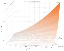
Compared to NMOS logic , double the number of transistors must always be applied to a chip, since the operating resistance of the NMOS implementation in CMOS is replaced by a PMOS transistor. The PMOS transistor is easier to integrate into ICs than a resistor . A resistor also produces unwanted heat as long as the transistor is conductive. Since there is no need for resistors in CMOS technology, in contrast to NMOS technology, there is an advantage: The current (from the supply voltage to ground) only flows at the moment of switching. (With the NMOS implementation there is the problem that in the conductive state “the strong zero” (0) from below has to prevail over “the weak one” (H) from above (see IEEE 1164) and thus a continuous current of flows at the top as long as the transistor remains conductive.) The current consumption or the power loss is therefore - apart from the much smaller leakage current - only dependent on the switching frequency (clock frequency) and the signal-to-noise ratio. For this reason, most binary integrated circuits ( processors , RAM ) are currently manufactured using this technology. The power loss is also linearly dependent on the clock frequency and quadratically on the signal-to-noise ratio (see graphic).
In analog applications, the high degree of integrability and capacitive control that MOSFETs make possible are used. By saving the resistors and using active loads (current mirrors as sources or sinks), noise dependencies and other undesirable effects can be reduced to a minimum. Due to the large frequency bandwidth of the components with high integrations, very broadband circuits can be created.
properties
The power loss in the idle state is usually approx. 10 nW, the power loss when switching is depending on the frequency and operating voltage, depending on the type of standard series, approx. 1 mW / MHz (integrated gates : approx. 10 µW / MHz).
In contrast to logic modules of the TTL family, which only work with 5 V, the typical operating voltage is between 0.75 and 15 V.
CMOS inputs are sensitive to static charges and overvoltages, which is why one or two-stage protective circuits are placed in front of CMOS inputs, if technically possible. For example, diodes against the two operating voltages or special protective circuits such as GgNMOS are provided. Furthermore, with CMOS circuits and with overvoltages at the inputs, there is the problem of so-called “ latch-ups ”.
Special types
HC / HCT-CMOS
Under HC-CMOS technology (H stands for High Speed ) is the advancement of CMOS logic 4000 family , to the speed of LS-TTL family to achieve. However, HC inputs are not fully compatible with TTL output levels. This is why HCT-CMOS technology was developed, in which the CMOS transistor structure was adapted to the output voltage levels of the TTL family with full pin compatibility with them. Mixing TTL circuits with HCT CMOS circuits within one circuit is therefore possible without restrictions.
BiCMOS
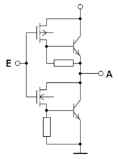
Under the BiCMOS technology is understood to mean a circuit technique in which field effect transistors with bipolar transistors are combined. Both the input and the logical link are implemented in CMOS technology - with the corresponding advantages. However, bipolar transistors are used for the output stage. This brings with it a high current drive capability and a low dependence on the capacitive load. For this purpose, two additional transistors and two resistors are usually required in the circuit in logic circuits. The input behavior corresponds to a CMOS circuit, the output behavior to a TTL circuit.
With BiCMOS it is still possible to combine logic circuits with power electronic circuit parts on one chip . Examples are switching regulators that can be operated directly on the rectified mains voltage .
application areas
Due to its low power requirement, CMOS technology is particularly suitable for the production of integrated circuits. These are used in all areas of electronics, for example digital clocks or in automotive electronics. It is also used to manufacture storage elements, microprocessors and sensors ( e.g. photo detectors in the form of CMOS sensors for digital photography or spectroscopy ).
CMOS technology is also used in analog applications. CMOS operational amplifiers are available which are characterized by an extremely high input resistance and low supply voltage.
See also
Individual evidence
- ^ Frank Wanlass , Chih-Tang Sah : Nanowatt logic using field-effect metal-oxide semiconductor triodes . In: 1963 IEEE International Solid-State Circuits Conference (February 20, 1963). Digest of Technical Papers . Vol. 6, 1963.
- ↑ Patent US3356858 : Low stand-by power complementary field effect circuitry. Registered on June 18, 1963 , inventor: Frank M. Wanlass.
- ↑ An Introduction to and Comparison of 74HCT TTL Compatible CMOS Logic ( Memento of the original from September 24, 2013 in the Internet Archive ) Info: The archive link was inserted automatically and has not yet been checked. Please check the original and archive link according to the instructions and then remove this notice. (PDF; 85 kB) Retrieved March 5, 2013
- ↑ László Palotas: electronics engineers . Vieweg + Teubner Verlag, 2003, ISBN 3-528-03915-9 , pp. 317 ff .

