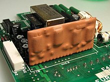
Thick-film hybrid technology

The thick-film hybrid technology is a construction and connection technology for the production of electronic circuits (thick-film hybrid circuit) in which both integrated and discrete components are used. The thick-film technology is generally also for the production of integrated therein or discrete resistors and trimming potentiometers used.
Procedure

As support material usually serve plates of alumina ceramic substrate , or (for the LTCC technology English Low Temperature Co-fired Ceramics ) and low-sintering ceramic films. Conventional FR-4 circuit boards made of glass fiber reinforced epoxy resin cannot be used because the temperature resistance is too low. In addition, aluminum oxide ceramics have a lower dielectric loss factor and a higher thermal conductivity than FR-4 or other circuit board materials, which is often a criterion for using thick-film technology.
The printed conductors are applied using the screen printing process and may also cross - by means of insulating layers . Similarly, electrical resistors produced which optionally subsequently through the laser trimming are subjected to a fine adjustment. Capacitors are also printed less frequently - however, only small values (<1 nF) can be produced.
The carrier printed in this way is burned, whereby the applied frits (powder mixtures for resistors, insulation or conductor tracks) fuse to form very resistant and reliable layers.
This thick-film circuit can then be equipped with further components that cannot be produced by printing technology, such as active components or electrolytic capacitors . The use of semiconductor chips without a housing ( bare chip assembly ) is recommended due to the good thermal conductivity of the carrier substrate. The most common connection techniques for the components attached to the carrier material are reflow soldering and chip and wire bonding.
For technological reasons, the component tolerances are originally high, but resistances can be adjusted later. The adjustment has a negative impact on the stability and climatic conditions.
advantages
- Use of components from different manufacturing techniques possible
- Substrate is a good, low-loss insulator
- Power loss is dissipated well via the substrate (approximately the same temperature over the entire circuit)
- Resistances that can be realized with printing technology of the highest accuracy (laser calibration, better than 0.1%) in wide value ranges (milli- to mega- ohm )
Areas of application

The fact that thick-film circuits can only be produced economically in larger quantities is an assertion that is no longer tenable these days, but should - depending on the application and intended use - be checked whenever a conventional solution in SMD technology on a printed circuit board presents technical difficulties brings.
The technical advantages of a hybrid circuit are undisputed, especially with regard to the factors miniaturization (available space for electronics), thermal conductivity , higher operating or ambient temperatures and other more extreme environmental conditions (e.g. vacuum).
Thick-film circuits are used wherever high reliability is required and / or adverse environmental conditions ( humidity , vibration ) prevail:
- Automotive electronics : (engine control, ABS, charge regulator etc.)
- Industrial and power electronics
- Science of measuring and control engineering
- Heavy -duty sensors (e.g. lambda probe )
- Military and aerospace engineering
- telecommunications
- High performance computer systems
- Consumer electronics ( low frequency - output stages of medium power)
- High-frequency - components (eg. The antenna amplifier and small transmitter)