
Memory module
A memory module or memory bar is a small circuit board on which several memory components ( dynamic RAM in the form of integrated circuits ) are soldered . Memory modules form or expand the main memory of electronic devices such as computers or printers and are plugged into specially designed slots .
The term memory module is seldom used for memory cards or USB sticks .


Designs
Commercially available module designs for personal computers are or were:
-
Single Inline Memory Module (SIMM) (This has only one row of lines, each of which is represented by a contact on both sides):
- 8 bit wide modules (30 contacts)
- This was also available in a variant with connection pins; it is referred to as a Single Inline Pin Package (SIPP), and practically corresponds to a SIMM with connecting pins soldered to the contact surfaces.
- PS / 2 SIMMs , 32 bit wide, 72 contacts, equipped with
- 8 bit wide modules (30 contacts)
-
Dual In-line Memory Module (DIMM) (Here the contacts on both sides are independent of each other.), 64 bit wide, equipped with:
- Synchronous Dynamic Random Access Memory ( SDRAM , SDR)
- Double Data Rate ( DDR-SDRAM , DDR)
- Double Data Rate 2 (DDR2-SDRAM, DDR2 )
- Double Data Rate 3 (DDR3-SDRAM, DDR3 )
- Double Data Rate 4 (DDR4-SDRAM, DDR4 )
- Small Outline Dual Inline Memory Module ( SO-DIMM ) for less space requirements (e.g. in notebooks )
- Micro Dual-Inline Memory Module ( Micro-DIMM )
- Rambus Inline Memory Module ( RIMM ), 16 bit wide
- Small Outline RIMM ( SO-RIMM )
There are a large number of manufacturer-dependent module forms (e.g. for servers ) and those for special requirements, including DIMMs with EDO RAM. On the other hand, other device types ( printers , RAID controllers) use common PC modules.
SIMM memory modules (asynchronous) are “ unbuffered ” or “ buffered ”, DIMM memory modules (synchronous, SDR, DDR) are “ unregistered ” or “ registered ”. As a further development of the registered modules, DDR2 and DDR3 modules have been introduced as Fully Buffered DIMM (FB-DIMM).
Buffered modules (buffered, registered, fully-buffered) are one clock cycle slower when accessed due to the latency of the buffer , but the electrical load on the memory interface in the chipset or in the CPU is reduced. This makes such modules, especially for server applications with a large memory expansion, useful due to a higher number of memory modules.
Parameters of a memory
Storage capacity (size)
The storage capacity of a memory module is usually the product of the storage capacity of the mostly similar memory chips and their number.
An example is a memory module that is equipped with 16 GM72V16821CT10K chips. The data sheet shows that this chip is organized in two banks of 524,288 (= 2 19 ) words each with a word length of 16 bits (2 × 2 19 × 16). This results in a storage capacity per chip of 2 × 2 19 × 16 bits = 2 24 bits = 16,777,216 bits. With 16 of these chips, the memory module has a storage capacity of 2 28 bits = 268,435,456 bits or - with 8 bits per byte - 2 25 bytes = 33,554,432 bytes = 32 MiB.
Some memory modules have one or two additional chips (of the same or a different type) that are responsible for error correction or parity functions. Here, 9 bits are often used for a byte (8 data bits and 1 check bit).
cables
The now outdated DDR / DDR2 memory has 64 data signal lines (or 72 for ECC ). The individual SDRAM chips are interconnected in such a way that they occupy the entire width of the data bus. Each chip is responsible for certain data lines. A chip with an “× n ” organization can supply n data lines. For a data bus with 64 lines, 64 / n chips with the organization “× n ” are required. For modules with several banks (see below) several chips (2 or 4) are connected in parallel on the data lines. Hence, a module with k banks contains 64 / n × k chips with the organization "× n ".
Additional input lines regulate the selection of the memory module ( Chip Select ) and the writing or reading direction (R / W) of the data.
speed
As with size, a distinction is made between the entire DIMM and the individual chips in terms of speed. A single chip always refers to the maximum clock frequency (for example DDR2-1066, DDR-400, SDRAM 133).
With the DIMM as a whole, however, it is about the data transfer rate (for example PC2-4200, PC3200). Equipped with SDRAM chips with DDR2-533, which have a clock frequency of 266 MHz, they transmit 4 data words per clock in DDR2 mode, and the maximum transmission rate can be calculated as follows, for example:
- 64 lines per memory module can transmit 4 × 8 bytes = 32 bytes per cycle;
- 133.3 million clock cycles / s (MHz) × 32 bytes = 4.266 billion bytes / s, or about 4.2 GB / s.
The data transfer performance value is only an ideal value and is never achieved in practice. However, it is common for classifying memory; in the example above it would be PC2-4200 made of DDR2-533 chips that run at 133 MHz (see DDR2-SDRAM ).
Benches / ranks
A DIMM can be built with a different number of identical modules. The JEDEC committee makes very specific requirements for the structure of the DIMMs. It is allowed to use chips that use either 4 (only with buffer), 8 or 16 data lines (see above lines). Furthermore, a specific group of DRAM chips is always assigned to a bank. A bank or a rank (according to JEDEC terminology) is a unique, independently addressable 64 bit wide area of a memory module (72 bit for ECC modules). Each bank behaves like a separate memory module. For this reason, two-bank modules, for example, place as much load on the bus lines as two single-bank modules. There are memory modules with one bank, two or four banks (single, dual and quad-rank DIMMs). Since chipsets can usually only manage a maximum of 8 banks (or at high speeds like DDR-400 usually only 6 banks), you have to use one-bank for large memory expansion (e.g. 8 × 2 GiB = 16 GiB). Use modules because with two-bank modules with 4 × 2 banks, all 8 banks would already be occupied. In addition, the speed of the RAMs usually has to be reduced in such cases, for example from PC3200 to PC2700, as otherwise the interference on the lines becomes too great.
There is no direct relationship between the number of banks and the one -sided or double-sided equipment of the memory modules with memory chips ( single-sided / double-sided ); H. Modules populated on one side can contain two banks, and modules populated on both sides can contain only one bank.
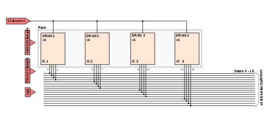
DRAM module with 1 bank:
The bank consists of 4 DRAM components and is activated via the ChipSelect signal.
DRAM module with 2 banks:
Each bank consists of 4 DRAM modules with 4 data lines (× 4) each.
The respective bank is selected for reading / writing via the ChipSelect 0/1 signals.

buffer
RAM chips are available with different bus widths (4 bit, 8 bit or 16 bit) and in different sizes (2015: 4 GBit, 8 GBit or 16 GBit). For the construction of small modules (2 GByte) a few small RAM chip components with a wide bus are required (4 pieces 256M × 16 bit). Each of these RAM chip modules is attached to the address and control lines (here are 4), and a RAM chip module is attached to the data lines.
For larger RAM modules, you usually first use larger RAM chip components (8 GBit, 16 GBit), then increase the number of components (8, 16, 32), using a narrower bus (8 bit, then 4 bits). In any case, the load on the address and control lines increases with the number of chips. If it exceeds 9, the address and control lines must be buffered; these modules are called RDIMMs. If the total bus width of all modules exceeds 64/72 bits, data lines must also be connected in parallel. This can make additional buffering of the data lines recommended or necessary; these modules are called LRDIMMs.
| Module size | Memory module | Fan-out | Remarks | ||
|---|---|---|---|---|---|
| number | Type (total) | Addresses | Data | ||
| 2 GB | 4 × | 256 M × 16 bit ( 4 GBit) | 4th | 1 | Smallest module with DDR4 RAM |
| 4 GB | 8 × | 512 M × 8 bit ( 4 GBit) | 8th | 1 | Expansion through more chips |
| 4 GB | 4 × | 512 M × 16 bit ( 8 GBit) | 4th | 1 | Expansion with a larger chip |
| 16 GB | 8 × | 2 G × 8 bit (16 GBit) | 8th | 1 | Fan-out of the addresses of 8, largest module available as unbuffered DIMM (UDIMM) |
| 16 GB ECC | 9 × | 2 G × 8 bit (16 GBit) | 9 | 1 | Version with ECC |
| 32 GB | 16 × a | 4 G × 4 bit (16 GBit) | 16 | 1 | Fan-out of the addresses of 16, requires buffering of the addresses (RDIMM: Registered DIMM) |
| 32 GB ECC | 18 × a | 4 G × 4 bit (16 GBit) | 18th | 1 | Version with ECC |
| 64 GB ECC | 36 × a | 4 G × 4 bit (16 GBit) | 36 | 2 | Fan-out of the addresses of 36, requires buffering of the addresses (RDIMM: Registered DIMM). Fan-out of the data from 2, if data is also buffered, it is (LRDIMM: Load Reduced DIMM). |
Registered DIMM and Load Reduced DIMM have higher latencies due to the additional latencies of the buffer modules.
How addressing works
The trigger for a write or read process in the main memory is mainly the CPU. Computer peripherals can also access the memory via DMA , but most operations are also initiated by the CPU.
If the CPU does not find data within the processor cache or wants to write data directly to the memory, the memory controller is instructed to do so. With older Intel CPUs such as B. the Pentium 4 or the Core 2 Duo, the commands are sent via the front side bus to the memory controller, which is located in the northbridge . Newer Intel processors such as models of the Core i series as well as AMD CPUs since the introduction of the K8 architecture have a significantly shorter route, since the memory controller is located directly in the CPU.
timing
There are a number of parameters that control the time behavior of the memory. By default, a time response set by the manufacturer is entered in the memory bar. With modern designs, there is an EEPROM on the latch that can be read by the BIOS and thus ensures correct configuration. So-called tuning by the user is often used to try to optimize this time behavior, but this can lead to system crashes.
DDR memory is labeled in the following way:
| speed | buffer | t CL | t RCD | t RP | SPD EEPROM version | PCB version |
|---|---|---|---|---|---|---|
| PC3200 | U | 30th | 3 | 3 | 1 | A1 |
In the above example a RAM is written with the parameters PC3200U-30331-A1. The most important parameter is the maximum speed of the module. "PC3200", as explained in more detail for speeds, denotes memory bars that can deliver 3.2 billion bytes per second. This makes it very easy to determine the assignment of processors / chipsets and suitable memory modules. An FSB-400 processor can also only send 3.2 GB / s via its interface. For this reason, this memory would therefore be sufficient for the corresponding processor. The “U” stands for unbuffered DIMMs. The important latency times follow after the hyphen, expressed in clock cycles:
- CAS Latency t CL : Duration between a read command and the receipt of the read data
- RAS-to-CAS Delay t RCD : (minimum) time between the activation of a line / bank and the sending of a read or write command.
- RAS Precharge Time t RP : (minimum) length of time between the deactivation of a line / bank and the reactivation of a line in the same bank.
With DDR-SDRAM there are chips with a CL of 2, 2.5 or 3 clock cycles, which is why you need two digits for the CL parameter (3033 stands for 3.0 - 3 - 3).
DDR2 memory is labeled in the following way:
| capacity | DIMM structure | speed | buffer | t CL | t RCD | t RP | SPD-EEPROM version | PCB version |
|---|---|---|---|---|---|---|---|---|
| 512MB | bRxc | PC2-3200 | U | 3 | 3 | 3 | 1 | A1 |
With DDR2 memory only integer times are allowed, which is why the CL is specified with only one number. In the JEDEC specification, the capacity size is only provided for DDR2 memory. Furthermore, information on the structure of the bolt is required. "1Rx8" stands for a single-rank DIMM, which contains (x8) SDRAMs (see bank ), each of which has 8 data connections.
Interesting parameters are also the operating voltage including the tolerance range, temperature limit values or other latency times such as t RAS or t RC . Such parameters are precisely defined in the JEDEC specification and are therefore not shown separately. The Activate-to-Precharge time t RAS is often given because it is interesting for overclockers. It is usually after t RP separated by a hyphen, e.g. B. PC3200-2022-5.
The command rate (1T / 2T) is also interesting for overclockers, although this latency of the memory chip is not an isolated property. This waiting time becomes necessary when many chips are active on the memory channel and the address lines of the memory controller are therefore more heavily loaded. As a rule, up to 3 ranks (a double rank and a single rank) can be addressed with 1T, with more you either have to lengthen the command rate or lower the clock frequency.
Important parameters for the time behavior of the storage tank are:
RAS-to-CAS-Delay - line operations
Column Address Select or Column Address Strobe , this control signal is present during a valid column address . The memory module stores this address in a buffer.
Synchronous DRAMs (SDRAM, DDR-SDRAM) also have the control inputs RAS and CAS , but here they have lost their immediate function. Instead, with synchronous DRAMs, the combination of all control signals (CKE, RAS, CAS, WE, CS ) are evaluated with a rising clock edge in order to decide whether and in what form the signals on the address lines must be interpreted.
The advantage of saving external address lines is offset by an apparent disadvantage in the form of delayed availability of the column address. However, the column address is only required after the row address has been decoded, a word line has been activated and the bit line signal has been evaluated. However, this internal process requires approx. 15 ns, so that the column address received with a delay does not have a negative effect.
RAS Active Time t RAS
The parameter t RAS (RAS pulse width, Active Command Period, Bank Active Time) describes the time that must have elapsed after activating a line (or a line in a bank) before a command to deactivate the line (precharge, Closing the bank) may be sent. The parameter is given by the fact that the amplification of the bit line voltage and the writing back of the information into the cell must be completely completed before the word line can be deactivated.
RAS Precharge Time t RP
The parameter t RP (Row Precharge Time) describes the minimum time that must have elapsed after a precharge command before a new command to activate a row in the same bank can be sent. This time is defined by the condition that all voltages in the cell field (word line voltage, supply voltage of the sense amplifier) are switched off and the voltages of all lines (especially those of the bit lines) have returned to their starting level.
RAS cycle time t RC
This describes the time between two total cycles, from the precharge to the precharge.
Error detection (ECC)
Memory modules can be used depending on the equipment
For simple error detection using parity bits, an additional bit is required for each 8-bit word width; the modules are consequently 9 bits (simple SIMM), 36 bits (PS / 2-SIMM) or 72 bits (common DIMMs). A single DIMM thus also offers enough bit width to use the error correction (see below), while several PS / 2 modules of the same type have to be connected in parallel for this purpose.
The error correction must also be supported by the motherboard (chipset and BIOS), the additional bits on the modules only create the possibility of storing the required information.
There are several methods of detecting main memory errors. One of these methods comes from the US mathematician Richard W. Hamming : The Error Correction Code (ECC) is a kind of hash value over the 64 bits of each memory line. This redundant information is calculated by the memory controller and stored in 8 more bits (with 32 bit memory lines there are 7 more bits), which is why the ECC memory has 72 bits per line. The process itself is called Error Checking and Correcting.
ECC can correct all 1-bit errors and detect all 2-bit errors as well as some multi-bit errors. ECC memory is rarely used in desktop PCs.
Other techniques for error detection are known under the names Chipkill, Active Memory, Memory Resiliency or Memory RAID.
The main cause of memory errors is not ionizing radiation (as previously assumed), but rather problems with individual memory cells (e.g. due to aging or manufacturing problems).
Comparison table
If a CPU (GPU, FPGA ...) has two, three, four or more memory interfaces, the data transfer speed can ideally double, triple, quadruple or multiply according to the number of memory interfaces. AMD's Athlon64-FX processor, for example, has two memory interfaces , whereas the Athlon64 in socket 754 has only one memory interface.
| Bus cycle | Bus width | designation | Data rate | |
|---|---|---|---|---|
| DDR SDRAM |
133 MHz | 64 bit | PC2100 | 2.133 GB / s |
| 166 MHz | 64 bit | PC2700 | 2.667 GB / s | |
| 200 MHz | 64 bit | PC3200 | 3,200 GB / s | |
| DDR SDRAM2 |
200 MHz | 64 bit | PC2-3200 | 3,200 GB / s |
| 266 MHz | 64 bit | PC2-4200 | 4.267 GB / s | |
| 333 MHz | 64 bit | PC2-5300 | 5.333 GB / s | |
| 400 MHz | 64 bit | PC2-6400 | 6,400 GB / s | |
| DDR SDRAM3 |
400 MHz | 64 bit | PC3-6400 | 6,400 GB / s |
| 533 MHz | 64 bit | PC3-8500 | 8.533 GB / s | |
| 666 MHz | 64 bit | PC3-10600 | 10.667 GB / s | |
| 800 MHz | 64 bit | PC3-12800 | 12,800 GB / s | |
| DDR SDRAM4 |
800 MHz | 64 bit | PC4-12800 | 12,800 GB / s |
| 933 MHz | 64 bit | PC4-14900 | 14.933 GB / s | |
| 1066 MHz | 64 bit | PC4-17100 | 17.067 GB / s | |
| 1200 MHz | 64 bit | PC4-19200 | 19,200 GB / s | |
| 1333 MHz | 64 bit | PC4-21300 | 21.333 GB / s | |
| 1600 MHz | 64 bit | PC4-25600 | 25,600 GB / s | |
| RDRAM | 400 MHz | 16 bit | PC800 | 1,600 GB / s |
| 533 MHz | 16 bit | PC1066 | 2.133 GB / s | |
| 600 MHz | 16 bit | PC1200 | 2,400 GB / s | |
| 800 MHz | 16 bit | PC1600 | 3,200 GB / s | |
| 1066 MHz | 16 bit | PC2100 | 4.267 GB / s |
The data rate is only used for classification and therefore does not correspond to the user data rate.
See also
- Cartridge (cartridge)
- Semiconductor memory
literature
- Horst Völz : Storage as the basis for everything. Shaker Verlag, Düren 2019, ISBN 978-3-8440-6964-8 .
Individual evidence
- ↑ Memory ranks and Intel E7320 / E7520 chipset based servers ( Memento of the original from March 31, 2010 in the Internet Archive ) Info: The archive link was inserted automatically and has not yet been checked. Please check the original and archive link according to the instructions and then remove this notice. (PDF; 278 kB). Kingston Technology memory ranking technical brief, April 2005.
- ↑ Corsair DDR2 FAQ ( Memento of the original from October 11, 2006 in the Internet Archive ) Info: The archive link was inserted automatically and has not yet been checked. Please check the original and archive link according to the instructions and then remove this notice. (PDF; 80 kB), February 2004. What's the difference between a rank and a bank?
- ↑ https://www.micron.com/products/dram/ddr4-sdram
- ↑ heise.de Main memory errors much more often than previously assumed (2009)
- ↑ cs.toronto.edu (PDF; 284 kB) DRAM Errors in the Wild: A Large-Scale Field Study, May 2009.
Web links
- Storage links and FAQs , heise.de
- RAM / main memory - RAM , CPU + mainboard FAQ, dch-faq.de
- Memory module - RAM glossary and FAQ , CompuRAM, Munich