
Bipolar transistor
A bipolar transistor , also known as a bipolar junction transistor (BJT), is a transistor in which, in contrast to the unipolar transistor , both types of charge carriers - negatively charged electrons and positively charged defect electrons - contribute to the current transport through the bipolar transistor. The BJT is controlled by an electric current and is used to switch and amplify signals without any mechanically moving parts.
Bipolar power transistors are designed for switching and amplifying signals with higher currents and voltages.
Historical
The idea of a “current-amplifying” or current-switching component based on semiconductors was already described by Julius Edgar Lilienfeld in the 1920s . Lilienfeld described an electronic component that is based on the phenomenon later called "field effect", ie a change in the conductivity of a material in the presence of an electric field, and which today is comparable to the field effect transistor . More or less independently of this, numerous other groups researched electrical effects in solids in the 1930s and 1940s. Theories on doping materials already existed, but the field effect transistor was not initially implemented (cf., among others, WR Brinkman et al., IM Ross or B. Lojek).
One of these research groups was Mervin Kellys' semiconductor group at Bell Laboratories in the 1930s , which was re-established after World War II in 1946 under the direction of William B. Shockley and Stanley Morgan . She also pursued the realization of a field effect component using silicon and germanium . During this time, John Bardeen gained important insights into understanding field effects. He recognized that even a relatively small number of surface states can hide changes in the charge in the semiconductor and thus prevent the implementation of a field-effect component. Together with other members of the group, especially Walter Brattain , he investigated how to clean the surface in order to reduce the effects of such surface conditions. As part of this development, Brattain observed a voltage gain of 15 for the first time on December 16, 1947. In his experiment, he cut off the tip of a polystyrene wedge coated with gold , so that two gold contacts lying close together were created. By pressing this wedge onto a germanium crystal, the first tip transistor was created . After another test on an oscillator on December 23 with HR Moore in the presence of RB Gibney, J. Bardeen, GL Pearson, W. Shockley, W. Brattain, H. Fletcher and R. Bown, he presented the component to management the following day in front. Shockley, Bardeen, and Brattain received the Nobel Prize for their discovery of the transistor effect and further work in this area.
Another important advance was made by Gordon Teal and Morgan Sparks at Bell Labs in the early 1950s when they developed a manufacturing process to manufacture bipolar transistors in the form of junction transistors with a grown / grown pn junction from a crystal (see pulled transistor ). . The first examples were presented by Bell Labs in 1951. The basis was still germanium, the first commercially available silicon junction transistors were developed by Teal in 1954 at Texas Instruments , with parallel work being carried out independently by Morris Tanenbaum at Bell Labs.
Types and symbols
Bipolar transistors are divided into npn and pnp types. The letters indicate the order and the doping type of the layering. A bipolar transistor thus essentially always forms two pn junctions connected against one another (similar to that in a pn diode ). The three connections are called the collector ( C , collector ), base ( B , base ) and emitter ( E , emitter ).
In the case of the pnp transistor, the order of the layers is pnp, i. This means that the two diodes between the base and emitter and between the base and collector each have the opposite polarity compared to the npn type.
In the circuit symbol is pressed from this difference by the directional arrow of the base-emitter diode turns.
In order to be able to remember the direction of the arrow of the circuit symbol better, there are two memorable sayings: "If the arrow hurts the base, it is about pnp" and "arrow to plate".
The direction of the arrow can also be explained with the technical direction of the current , which always runs from plus to minus. The arrow is always on the emitter side and points in the direction in which the positive charge carriers are moving. In the case of the npn transistor (negative-positive-negative), the arrow points outwards, there is also a saying for this: "If the arrow wants to separate from the base, it's npn."
The diode circuit shown in the equivalent circuit does not produce a transistor effect, because the charge carriers would recombine in the area of such a pseudo base. This also applies to structures in which the distance between the emitter-base and collector-base zones is too large, i.e. i.e., the base zone is too thick. For the formation of the transistor effect, the condition must be met that the base thickness is smaller than the diffusion length ( W muss L b ).
construction
The bipolar transistor is a combination of three alternating p- and n-doped semiconductor layers (npn and pnp). These oppositely connected pn junctions must be close together in order to realize the transistor function.
The three differently doped areas are called collector (C), base (B) and emitter (E). The base is particularly thin and lies between the collector and emitter. Note the different doping in the bipolar transistor. The emitter is more heavily doped than the base, which in turn is more heavily doped than the collector. This asymmetrical structure causes a different behavior in normal and inverse operation.
The first bipolar transistors were made from an n-doped semiconductor wafer, into which the emitter and collector zones were introduced from both sides by diffusion of p-dopants until there was only a small distance inside the wafer between these p-doped regions. The two-sided contact was made by wires, while the base connection was formed by the semiconductor chip itself (hence the name base).
As a result of optimizations, bipolar transistors are nowadays made up of more than three layers; the additional layers are not composed in the form of further pn junctions, but rather the three main layers are divided into zones of different doping density. The collector zone always consists of at least two differently doped zones. Usually, a metal contact is doped more highly in order to reduce the effect of a Schottky diode . The designations npn and pnp only refer to the active inner area, not the actual structure.
- Bipolar transistors in epitaxial - planar technology
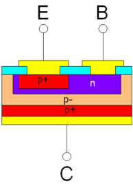
schematic structure
(pnp transistor)
schematic structure
(npn transistor)
practical structure
(npn transistor)
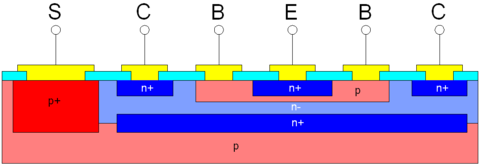
Today, single transistors are mostly manufactured using the epitaxial planar design. Integrated transistors are also manufactured in epitaxial planar design, but the collector connection is located on the top. The substrate connection (S) is a connection with the deeper layers. A negative voltage is applied to the substrate connection. This causes the substrate diode to be blocked and the individual transistors to be separated.
In the case of integrated transistors, a fundamental distinction is made between vertically and laterally constructed transistors. In practice, npn transistors are constructed vertically and pnp transistors laterally. Vertical transistors have a vertical current flow. In the case of lateral transistors, the current flow is horizontal, and the current gain is 3 to 10 times greater, and the switching frequencies are higher because the base zone can be made smaller. For this reason, npn transistors can also be constructed laterally, then all p- are replaced by n- and n- by p-zones; the same applies to the doping of the substrate, which is connected to a positive voltage.
Pairs of npn and pnp transistors are called complementary if their electrical data are similar except for the sign. Such "transistor pairs" selected for a good match of the parameters (current amplification and base-emitter voltage are decisive) are e.g. B. used in so-called push-pull circuits such as amplifier output stages to keep distortion low.
If large currents are required, several transistors can be connected in parallel. The correspondence of their parameters is also important here, but emitter resistors must be used to ensure that the currents are evenly divided between all parallel transistors.
schematic structure
(integrated vertical npn transistor)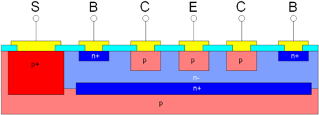
schematic structure
(integrated lateral pnp transistor)
Semiconductor components that are made up of more than three layers (e.g. pnpn) have more than one static state of current flow. These include four-layer diodes ( thyristors , diacs ) and triacs .
see also: Manufacturing of integrated circuits
functionality
A bipolar transistor consists of two pn junctions, which is why there are four possible types of wiring, since each pn junction can be switched in forward or reverse direction. The most common type of wiring is the amplification area, where the emitter-base transition is polarized in the forward direction and the base-collector transition is polarized in the reverse direction.
An electrical current I B between the base and emitter controls a higher current I C between collector and emitter. The ratio of the two currents, which is in the range from about 4 to 1000, depends on the transistor type and the absolute amount of the collector current and is referred to as the static current amplification factor B.
This behavior is comparable to a flow-dependent valve in a water channel model. This model is highly simplified and only serves to illustrate the general currents flowing because of the bipolar transistor both electrons and to explain the real situation and the operation holes are responsible (holes).
In the following, the general mode of operation of a bipolar transistor in forward operation ( U BE > 0, U CB > 0) is shown using the example of an npn transistor .
If only the collector and emitter are connected (voltage U CE > 0), this corresponds to two diodes connected in opposite directions, one of which (the base-collector diode) is always blocked. Only a small current flows, the amount of which is equal to the reverse current of the base-collector diode. The applied voltage reduces the base-emitter barrier layer , the space charge zone (RLZ) between base and emitter, but increases the base-collector barrier layer.
By closing the base-emitter circuit (voltage U BE > U D (U D corresponds to the diffusion voltage ), for silicon U BE > 0.7 V), the base-emitter diode becomes conductive. As with the simple pn diode, holes are injected from the base (p-doped) into the emitter (n-doped ). A small base current I BE1 flows . In the emitter region, the excess of minority charge carriers, in this case holes, decays with the diffusion length , and the holes recombine with the electrons. Similarly, electrons from the emitter (Latin: emittere = to send out) are injected into the base. Since the emitter is more heavily doped than the base, the flow of electrons from the emitter to the base predominates. This electron flow is much greater than the hole flow from the base into the emitter. Due to the small width of the base, which must be smaller than the diffusion length of the charge carriers, only a few of the electrons recombine with the hole. Most electrons (approx. 99%) diffuse through the base into the collector-base barrier, the base-collector junction is operated in the reverse direction. There they drift into the collector (lat. Colligere = collect) because of the large drop in potential ( U CB > 0 ). In the form of the collector current I C , electrons thus flow from the emitter into the collector.
The number of electrons injected into the base region or the defect electrons injected into the emitter changes with the forward voltage U BE of the base-emitter diode. Although only a relatively small number of electrons recombine in the base, this part is essential for the function of the bipolar transistor. A large number of electrons increases the likelihood that an electron will hit a hole and recombine. The recombining defect electrons are supplied via the base contact in the form of part of the base current. By changing the base current I B , the collector-emitter current I C can accordingly be controlled. A much larger collector current (electron current) is controlled by the small base current caused by the holes in the hole.
However, this control is asymmetrical in its behavior. While an increase in the base current quickly enables the collector-emitter current, it takes longer for the above. Processes cease and the component returns to equilibrium with less electricity. This duration is heavily dependent on the previous ratio of base current to collector current. If more charge carriers are available than are necessary for the collector current (saturation), this further delays the shutdown. In saturation there is no control of the collector emitter current, since the base current is not the limiting factor. With rapid shutdown, a negative base current can flow for a short time at the same time as a decreasing collector current. This behavior also applies to the pn diode , the blocking delay time. Since the pn diode without a base cannot lead to an oversupply of charge carriers, it switches off much faster than a bipolar transistor. With rapid changes in the base current or in saturation, the approximation of the constant current gain does not apply. This switch-off delay is the main reason why the fastest discrete bipolar NPN silicon epitaxial transistors reach a cut-off frequency of 1 GHz at best. The heterojunction bipolar transistor is a clear improvement .
Another limiting factor that has to be overcome in terms of circuitry is the Miller effect or the capacitance between collector and base. In the case of small-signal transistors, this is a few pico-farads. If the collector potential changes, a charge-reversal current flows through C CB and the base. This current is amplified and counteracts the change in potential. The decoupling of the collector current of an emitter circuit by a base circuit avoids this effect, since the input resistance of the base circuit is almost zero. A narrowband solution is the parallel compensation of C CB with an inductance.
The mode of operation of a pnp transistor is analogous to this, but the signs have to be reversed in order to take into account the opposite doping of the two barrier layers. The base current corresponds to a small electron current, which causes a high current of holes from the emitter into the collector.
In the overview below, the relationships are shown schematically as a ribbon model in the crystal. The small ± symbols represent mobile charge carriers, the majority charge carriers such as electrons or holes, while the large symbols represent the ionized doping atoms.
- Ribbon model for the bipolar transistor (npn type)
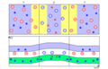
Crystal structure and ribbon model of a bipolar transistor
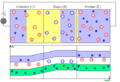
Same with applied collector-emitter voltage

Additionally with applied base-emitter voltage
Transistor models and equivalent circuit diagrams
The bipolar transistor is a very well researched component. There are numerous models to describe its behavior that facilitate circuit analysis and design. Since the detailed descriptions are very extensive, only the basics are touched on here and more in-depth information is split up into sub-articles. See the mathematical description of the bipolar transistor and equivalent circuits of the bipolar transistor , further transistor noise in the form of Johnson noise at real resistances and shot noise due to the leakage current .
The simplest model consists of the base-emitter diode, and by the base current I B -controlled current source (more specifically, a current sink , since no energy is generated) from the collector to the emitter I C . The transistor amplifies the base current by a factor of B. Requirements for the validity of the model are: The base-emitter diode must be polarized in the forward direction and the base-collector diode in the reverse direction.
This type of description is called the large-signal model and is divided into the Ebers-Moll model, the transport model and the Gummel-Poon model.

The disadvantage of the methods mentioned above is the use of non-linear functions in the form of the exponential function for the diode characteristic, which makes mathematical analysis difficult. The small signal model provides a remedy . It can be used to apply the theories that apply to linear circuits.
The parameters are determined at the operating point, i.e. under defined boundary conditions. The differential resistance of the base-emitter path r BE corresponds to the tangent to the diode characteristic for the operating point. The differential collector-emitter resistance r CE corresponds to the slope of the output characteristic due to the Early effect . The differential current amplification factor β completes the description of the electrical behavior. (The data sheet value h FE corresponds to β.)
The four-pole parameters of the transistor are directly related to the small-signal model .
The large-signal model covers the entire voltage range that is permissible for the component under consideration. The small signal model only applies in a narrowly limited area around the operating point. A further subdivision is made into static and dynamic models. The latter are more complex because they take into account the capacitive properties of the barrier layers and are therefore suitable for medium to high frequencies.
Characteristic curves
Characteristic fields are used to graphically represent two or more interdependent physical quantities. They serve to characterize and illustrate the electrical properties / behavior of the component. Four basic characteristics are sufficient to describe a bipolar transistor (as an electrical switch or in amplifier circuits): the input, output, current control and voltage feedback characteristic field. If the characteristics are shown together, one also speaks of a four-quadrant characteristic field.
In the input characteristic field, the base current is plotted against the base voltage . Since this is only the base-emitter-pn junction, the characteristic corresponds to that of a pn diode.


The output characteristic field shows the dependence of the collector current on the collector-emitter voltage for selected base control currents .


In the case of the current control characteristic field or the current control characteristic, the dependence of the collector current on the controlling base current with a constant collector-emitter voltage is shown. As a rule, it has the shape of a straight line (approximately linear) through the origin, with the gradient corresponding to the current gain factor.

The voltage feedback characteristic field (also called feedback characteristic field) represents the reaction of the output voltage on the input (base or base voltage ).
working area
The bipolar transistor consists of two pn junctions. By applying appropriate voltages, both transitions can be blocked or switched through independently of each other. This results in four possible working areas in which the transistor shows its own behavior.
Restricted area
In the stop band (engl. Cut-off region ) or locking operation to lock both transitions, d. H. the collector and emitter diodes. In this operating state, the transistor theoretically does not conduct any current. The transistor thus corresponds to an open switch. In practice, a small current also flows in blocking mode, so the transistor in blocking mode is a non-ideal switch.
Reinforcement area
The forward-active region occurs in so-called normal operation . The emitter diode is operated in the forward direction and the collector diode in the reverse direction. In the amplification range, the following formula applies approximately , where β is the current amplification factor. Since β is relatively large, small changes in the base current lead to large changes in the collector current . Transistors operate in this area to amplify signals. In normal operation, the transistor is usually only operated in the range in which the gain is approximately linear according to the above formula.


Fast digital circuits such as LVPECL , LVDS , CML work in amplification mode, also known as the linear range, in order to avoid the delays caused by saturation.
Saturation range
The saturation range is also called saturation mode or saturation . Both pn junctions are conducting, but there are more charge carriers in the base zone than are required for the collector current. The collector current is independent of the base current . The transistor corresponds to a closed switch with constant volume resistance (left area in the output characteristic field). If the operating point of a linear amplifier is not far enough away from the saturation range or the amplitude of the signal is too high, overdrive occurs, the amplifier limits the signal and distortions occur. The blocking of the base-collector section is delayed because all excess charge carriers have to flow out of the base zone first.
Alternatively, field effect transistors (e.g. MOSFETs ) are used in switching applications.
Quasi-saturation area
This range is between the gain range and the saturation range . The transistor is not operated in saturation, as a result of which the turn-off time and thus the turn-off power loss are significantly reduced compared to operation in full saturation, which is important for switching applications. However, this advantage is paid for by higher forward losses, since the forward voltage is approx. 0.4 V higher. One application is, for example, Schottky TTL .
Inverse gain area
The inverse gain region (English reverse region ) is also called inverse operation . The base-collector junction is operated in the forward direction and the base-emitter junction in the reverse direction. This range works similarly to the normal gain range, but with the opposite sign of the voltages. The current amplification factor is significantly smaller. The maximum reverse voltage of the base-emitter diode is only a few volts.
An advantage of the inverse operation is the more precise and faster switching. When fully controlled, the forward voltage drops below 10 mV, similar to mechanical contact, but without bouncing.
Embodiments
Electrical parameters
There are thousands of transistor types with different properties for different purposes. Important parameters are
- the current carrying capacity I C (collector current; a few milliamperes to approx. 50 amperes),
- the maximum voltage load U CE (collector-emitter reverse voltage; a few volts to a few hundred volts),
- the maximum power loss P max (a few milliwatts to a few hundred watts),
- the current gain B (approx. 5 to approx. 1000) and
- the cutoff frequency (approx. 10 kHz to approx. 100 GHz).

2N3055 from the 1980s. See the difference in manufacturing technology to the picture above: wire bonding technology, spacing of the lines

Performance Darlington from the 1980s

Often, in practice, a few types are used more often than others. Many transistors are available as complementary types: there is a pnp and an npn type with parameters that are the same in terms of amount, but different polarity. Some complementary types and their parameters are representative here:
- Small signal transistors (general application):
- TO-92 housing (wired): BC547B (npn transistor) / BC557B (pnp transistor): power loss P max = 0.50 W; Amount of collector current I C ≤ 100 mA; Amount of reverse voltage U CE ≤ 45 V; Current gain B ≈ 290 (at I C = 2 mA)
- SOT-23 package ( SMD ): BC817 (npn) / BC807 (pnp): P max = 0.25 W; I C ≤ 500 ... 800 mA; U CE ≤ 45 V; B = 100… 600 (at I C = 100 mA); Transit frequency F T (min.) 100 MHz
- The price of these types is around 3 ct for small quantities, and for larger quantities the price drops again significantly.
- Power transistors:
- TO-3 package : 2N3055 (npn) / MJ2955 (pnp): P max = 115 watts; I C ≤ 15 A; U CEO ≤ 60 V; B = 20… 70 (with I C | = 4 A); Transit frequency min. 0.8 MHz
- TO-220 housing, Darlington transistors : TIP130… 132 (npn) / TIP135… 137 (pnp); Collector currents up to 8 amps, current gain min. 1000 (at 4 amps collector current), reverse voltage 60 to 100 volts.
Darlington transistors combine two transistors on one chip in one housing, the smaller of which is used to control the base of the larger in an emitter follower circuit. The current gain of the double transistor is significantly higher (1,000 to 30,000) than that of a single transistor, but the saturation voltage is also (around 1 V). The BE voltage is roughly twice the value of a single transistor (1.4 V).
Housing designs
see also: List of semiconductor packages
Discrete bipolar transistors are housed in different housings depending on the purpose. The most common housing forms are:
- Wired housing ( through hole mounting , short THT from through hole technology ):
- TO-92 (plastic housing 5 mm × 5.2 mm)
- TO-18 and TO-39 (cup-shaped metal housing, encapsulated; outdated)
- TO-220 (plastic housing with tab for heat sink mounting, 9.9 mm × 15.6 mm)
- TO-218 (15 mm × 20.3 mm; plastic with metal cooling surface)
- TO-247 (plastic housing with metal surface for heat sink mounting)
- TO-3 (metal housing for heat sink mounting; outdated)
- TO-3P (similar to TO-218; with metal surface for heat sink mounting)
- Housing for surface mounting ( SMD of Engl. Surface mounted device ); Heat dissipation via solder connections to the circuit board :
See also
- Identification letters of semiconductor components
- Heterojunction bipolar transistor
- Basic transistor circuits
- IGBT (a mix of bipolar transistor and MOSFET )
- List of semiconductor packages
literature
- Ulrich Tietze, Christoph Schenk: Semiconductor circuit technology . 12th edition. Springer, Berlin 2002, ISBN 3-540-42849-6 .
- Stefan Goßner: Basics of electronics. Semiconductors, components and circuits . 11th edition. Shaker Verlag, Aachen 2019, ISBN 978-3-8440-6784-2 .
Web links
- Datasheet Catalog. Retrieved on September 21, 2009 (English, data sheet collection of electronic components).
- Philipp Laube: Structure of a bipolar transistor. In: halbleiter.org. 2009, accessed on March 6, 2016 (Basics and manufacturing steps for the production of bipolar transistors).
- How A Bipolar Transistor Works - Animated Model of a Bipolar Transistor
- Hansjörg Kern: Using a bipolar transistor. Retrieved March 13, 2013 (Using Bipolar Transistors, Circuit Examples, Bipolar Transistors, and Operational Amplifiers).
Individual evidence
- ↑ a b W. F. Brinkman, DE Haggan, WW Troutman: A history of the invention of the transistor and where it will lead us . In: IEEE Journal of Solid-State Circuits . tape 32 , no. 12 , 1997, p. 1858-1865 , doi : 10.1109 / 4.643644 .
- ↑ IM Ross: The invention of the transistor . In: Proceedings of the IEEE . tape 86 , no. 1 , 1998, p. 7–28 , doi : 10.1109 / 4.643644 ( PDF [accessed on January 28, 2013]). PDF ( Memento from February 1, 2012 in the Internet Archive )
- ↑ Bo Lojek: The MOS Transistor . In: History of Semiconductor Engineering . Springer, Berlin 2007, ISBN 978-3-540-34257-1 , pp. 317 ff .
- ↑ Bo Lojek: The MOS Transistor . In: History of Semiconductor Engineering . Springer, Berlin 2007, ISBN 978-3-540-34257-1 , pp. 18-20 .
- ^ GK Teal, M. Sparks, E. Buehler: Growth of Germanium Single Crystals Containing pn Junctions . In: Physical Review . tape 81 , no. 4 , 1951, pp. 637-637 , doi : 10.1103 / PhysRev.81.637 .
- ↑ The first silicon transistor was likely demonstrated by Morris Tanenbaum at Bell Labs in January 1954 , but Bell Labs did not patent it and kept the discovery a secret. For the history of the silicon transistor, see Silicon Transistor . IEEE, accessed January 24, 2014.