
Metal-oxide-semiconductor field effect transistor
The MOSFET ( English metal-oxide-semiconductor field-effect transistor , MOSFET and MOSFET , rarely MOST ) is one of the field-effect transistors with insulated gate , as IGFET called (see also section name ). It belongs to the metal-insulator-semiconductor field effect transistors (MISFET). Although doped polysilicon is the predominant gate material today, the name MOSFET has been retained.
As with all IGFET transistors, a MOSFET is controlled via a control voltage (gate-source voltage) or control potential (gate potential), with which the current flow from drain to source can be influenced.
Because of the high packing density and the low production costs, it is the most widely used transistor for analog and digital integrated circuits . In 2008 z. B. built into a processor alone up to 1.9 billion transistors.
history
The functional principle of MOSFETs is around 20 years older than that of the bipolar transistor . The first patent applications were made in 1926 by Julius Edgar Lilienfeld and in 1934 by Oskar Heil . However, the first MOSFETs were not manufactured until 1960, when silicon / silicon dioxide was a material system with which a reproducibly good semiconductor-insulator interface could be produced. Associated with this was the abandonment of germanium as the base material and increasing demands on the production conditions ( clean rooms , strict temperature regime).
From the beginning or mid-1970s, doped polysilicon was used as a gate material, thus displacing vapor-deposited aluminum . Since the turn of the millennium, research has been intensified on the new high-k + metal gate technology, and it was first used in mass production in 2007.
Surname
The name metal-oxide-semiconductor field effect transistor goes back to the original layer sequence of the gate layer stack. Until the early 1980s, the use of aluminum (a metal) as a gate material dominated, which was separated from the conductive channel in the silicon substrate (semiconductor) by a non-conductive silicon dioxide layer (insulator). In the 1980s, processes that used doped polysilicon as a gate material became increasingly popular . To this day, this is the most common type of commercially available CMOS circuit. Since no metal is used, the term MOSFET is no longer correct, but is still used as a synonym.
With increasing miniaturization, MOS transistors with a polysilicon gate show electrical disadvantages, because with certain circuits, a depletion area forms in the gate ( polysilicon depletion ). Therefore, research into alternative gate materials (e.g. transition metals ) has been carried out since the early 2000s . At the same time, research was also carried out into alternative insulator materials with a high dielectric constant (so-called high-k materials) in order to reduce the increasing leakage currents. In 2007, Intel was the first manufacturer to introduce a combination of both changes (cf. high-k + metal gate technology ); some other manufacturers of high-performance processors followed. In these cases the designation MOSFET is correct again, but it is often cheaper to use the neutral designation MISFET (metal-non-conductor-semiconductor-FET) or more generally IGFET (FET with insulated gate).
Structure and functionality
.svg)
A MOSFET is an active device having at least three terminals ( electrodes ): G ( gate , dt. Control electrode ), D ( drain , dt. Outflow ), S ( source , dt. Source ). In some designs, an additional connection B ( bulk , substrate) is led to the outside, which is connected to the back of the chip. Since a voltage on the back of the chip generates additional electrical fields that act on the channel, changing the voltage on the B connection shifts the threshold voltage of the MOSFET. Most of the time, however, the substrate is internally connected to the source.
Like other field effect transistors, the MOSFET acts like a voltage-controlled resistor, that is, via the gate-source voltage U GS , the resistance between drain and source R DS and thus the current I DS (simplified I D ) can be changed by several orders of magnitude through R DS become. The key to understanding this change in resistance in a MOS structure lies in the formation (enrichment types) or pinching (depletion types) of a conductive channel under the gate (details see below).
Basic types
Similar to the bipolar transistor , the MOSFET can be divided into the two basic variants p-type (also p-conductive, p-channel or PMOS ) and n-type (also n-conductive, n-channel or NMOS ). If both types are used together, for example in integrated digital circuits, one speaks of CMOS ( complementary MOS ). In addition, there are two forms of both variants that differ in their internal structure and electrical properties:
- Depletion mode (Engl .: depletion ) - also normally on , normally-on , normally conducting
- Enrichment type (English: enhancement ) - also self-locking , normal-off , normal locking
In practice, the vast majority of enrichment types (= normally blocking) are used.
Basic structure and physical function
The self-blocking n-channel MOSFET (enhancement type) is given as an example.
A weakly p- doped silicon single crystal (substrate) is used as the base material . Two heavily n-doped regions, which produce the source and drain connections, are embedded in this substrate. The substrate is still located between the two areas, creating an npn structure that initially does not allow any current to flow (compare npn transistor : without a base current, the transistor is blocked). A very thin, resistant insulating layer (dielectric, mostly silicon dioxide) is then applied precisely over this remaining space. The dielectric separates the overlying gate electrode from the silicon (more precisely from the channel region). Up to the mid-1980s, aluminum was used as the gate material, which was replaced by n + or p + -doped (degenerate) polysilicon (abbreviation for polycrystalline silicon).
As a result of this structure, the gate connection, dielectric and bulk connection form a capacitor which is charged when a positive voltage is applied between gate and bulk. As a result of the electric field, minority carriers (in p-silicon electrons) migrate to the boundary layer in the substrate and recombine with the majority carriers (in p-silicon defect electrons ). This has the effect of displacing the majority holders and is called "impoverishment". A space charge zone arises at the boundary layer to the oxide with a negative space charge. Above a certain voltage U th ( threshold voltage ), the displacement of the majority charge carriers is so great that they are no longer available for recombination. There is an accumulation of minority carriers, as a result of which the actually p-doped substrate becomes n-conductive close to the insulating layer. This condition is called strong " inversion ". The band model explains the increased gate voltage leads to a band bending of conduction and valence bands at the boundary layer. From the critical voltage onwards, the Fermi level is closer to the conduction band than to the valence band. The semiconductor material is thus inverted. The resulting thin n-conducting channel now connects the two n-regions source and drain, which means that charge carriers can flow (almost) unhindered from source to drain.

In principle, the source and drain connections are initially equivalent. Usually the structure is not symmetrical in order to achieve better behavior. In addition, in most designs, the bulk is electrically connected internally to the source, as a potential difference between source and bulk has a negative effect on the properties of the transistor (especially the threshold voltage) ( body effect ). This connection has no influence on the basic function. However, there is also a diode between the bulk and drain connections, which is parallel to the actual transistor. The bulk with the p-doped substrate and the drain with the n region form the pn junction . This inverse diode is shown as an arrow in the circuit symbol of the MOSFET. With the n-channel MOSFET, it points from the bulk connection to the channel.
Allocation of the source and drain areas for PMOS and NMOS
_with_currents_DE.svg)
Source refers to the connection from which the charge carriers responsible for charge transport (majority charge carriers) drift in the conductive case in the direction of the drain connection.
In the p-channel MOSFET (PMOS, PMOSFET), defect electrons (holes) form the majority charge carriers, they flow in the direction of the technical current direction . When connecting p-channel MOSFETs, the source potential (+, closer to ) is greater than the drain potential (-; closer to ).


In the case of the n-channel MOSFET (NMOS, NMOSFET), however, electrons form the majority charge carriers. They flow against the technical direction of the current. With regard to the electrical potential, the position of the source and drain is therefore opposite to that of the p-channel MOSFET. This means that the source potential (-; closer to ) is lower than the drain potential (+; closer to ).
variants
With the increasing demands on the electrical properties of MOSFETs and the need to deal with the effects of miniaturization in transistors (e.g. short channel effects ), variants of the planar MOSFET have been developed over the past decades. They often differ in the design of the doping profile or the choice of material. Examples are LDD MOSFETs (from English lightly doped drain ), transistors with halo implants or stretched silicon, and HKMG transistors . Since, as a rule, different improvements are used at the same time, no classification can be used here.
In addition, a distinction must be made between lateral (i.e. aligned parallel to the surface) and vertical designs. While lateral transistors are mainly used in communications technology ( lateral double-diffused MOSFET , LDMOS), the vertical design is mainly used in power electronics. The advantage of the vertical structure is the higher possible reverse voltage of the components.
Circuit symbols
In the German-speaking countries, representations with the four connections for gate, source, drain and body / bulk (central connection with arrow) are mostly used as circuit symbols . The direction of the arrow on the body / bulk connection indicates the type of channel, i.e. the type of majority charge carrier. Here, an arrow to the channel indicates an n-channel transistor and an arrow away from the channel indicates a p-channel transistor. Whether the transistor is normally-off or normally-on is shown by a dashed ("channel must first be inverted" → enrichment type, normally-off) or a continuous ("current can flow" → depletion type, normally on) channel line. In addition, other symbols are common, especially in the international environment, in which the body / bulk connection usually connected to source is not shown. The transistor type is then again identified using arrows and various symbolic representations of the channel and a circle on the gate, cf. Table. To identify the source electrode, in some symbols the contact to the gate is not shown in the middle above the channel, but directly opposite the source connection.
Circuit symbols of discrete MOSFETs (selection of different representation variants) Line /
channel typeType of enrichment
(self-locking)Impoverishment type
(self-conducting)p-channel 


n-channel 


Characteristic field
| symbol | calculation | description |
|---|---|---|
| Output voltage between drain and source | ||
| Input voltage between gate and source | ||
| Voltage between source and back gate, also known as the bulk connection |
||
| positive supply voltage from NMOS, is also used in CMOS technology |
||
| negative supply voltage from NMOS, is also used in CMOS technology |


Threshold voltage
The threshold voltage (ger .: threshold voltage ) is a key element in the model consideration of MOSFETs and depends strongly on the process from. The doping of the source, drain and the channel region determines the size of the threshold voltage.

- for NMOS depletion type and PMOS enrichment type
- for NMOS enrichment type and PMOS depletion type, typ. between 1 V and 3 V.


In addition, the threshold voltage is dependent on the temperature. The 1st order dependency is sufficient for the description (linear dependency):

where is the temperature coefficient, the temperature and the support temperature (e.g. the typical operating temperature).


Output characteristic field

The representation of the relationships between the drain current (also called drain-source current) and the drain-source voltage as a function of the gate-source voltage is referred to as the output characteristic field of a MOSFET. It is basically the same for all MOSFETs (NMOS enhancement type, NMOS depletion type, PMOS enhancement type and PMOS depletion type). There are only differences in the potential reference points of drain and source and in the sign of the gain factor. The characteristics are influenced by other effects (temperature, substrate bias , short channel effects, etc.).


The individual I D - U DS characteristic of a MOSFET is divided into three areas: the blocking area, the active area and the saturation area.
Restricted area
In the stop band (engl. Cutoff region ), also cut-off or sub-threshold region (engl. Subthreshold region ) called the gate-source voltage is below the threshold voltage .
The following applies to:


With
- the threshold voltage current (engl .: threshold current )
- the subthreshold swing (reciprocal of subthreshold slope , subthreshold slope )
- the temperature stress ,
- the Boltzmann constant ,
- the charge of the charge carriers involved (≙ elementary charge ),
- the emission factor in the sub-threshold region (engl. sub-threshold slope factor ) and
- the depletion capacitance (ger .: depletion capacitance ), this consists of the overlap capacitances at the drain and source


The leakage current of an enhancement MOSFET is calculated from the equation for the blocking range:
- (only for NMOS enhancement and PMOS enhancement types).

Linear area
In the linear area (also called triode area, ohmic area or active area, English: ( triode region or ohmic region )) the gate-source voltage is above the threshold voltage (in the case of the enhancement MOSFET), so that a continuous channel between the drain and Source is created. The range is limited by the characteristic curve of the limit voltage.

The name comes from the fact that the characteristics run almost linearly through the origin, which corresponds to the behavior of an ohmic resistor .

For and applies:


With
- the NMOS gain factor (n-doped) ,
- the PMOS gain factor (p-doped) ,
- the charge carrier mobility of the electrons in n- or p-doped substrate or
- the area-specific capacitance of the gate capacitor
- the width and length of the gate,
- the thickness of the gate dielectric,
- the permittivity of the respective material, e.g. B. silicon as substrate and silicon dioxide as dielectric,


Saturation range
In the saturation region , active mode , the I DS - U DS characteristic curve runs approximately parallel to the axis. That is, if the voltage between drain and source is increased, this hardly has any increasing effect on the current that flows between these contacts. The limit from which this behavior becomes apparent is defined as. As can be seen in the output characteristic field, the input voltage can be used to influence the current directly. In this case the transistor behaves like a current source controlled by the input voltage . Further effects arise from the channel length modulation .

If the input voltage at the transistor is above the threshold voltage:
- ,
and the output voltage is above the saturation voltage (or pinch-off voltage):

then applies to the current in the output circuit:


When making a comparison with a bipolar transistor, when using the term saturation range, it must be noted that the term saturation has a different meaning for the bipolar transistor.
Characteristic effects
Substrate bias, back gate control, body effect
When a substrate bias (also known as back-gate voltage) is applied to the transistor, the threshold voltage depends on the source-bulk voltage . The larger the voltage becomes, the larger the threshold voltage becomes.

With
- the substrate effect parameter ,
- the surface potential at strong inversion: ,
- the doping concentration of the substrate or the n- or p-well (typical values are in the range 10 13 to 10 17 cm −3 ) and
- the intrinsic conductivity concentration of the undoped (intrinsic) substrate material (e.g. 10 10 cm −3 silicon at room temperature).


Channel length modulation
The term channel length modulation is understood to mean an effect that is similar in its effects to the Early effect of the bipolar transistors. The channel length modulation occurs in the saturation area ( ) and models the constriction of the channel (the channel no longer reaches the drain, the region without a channel is also called the pinch-off region). The channel length modulation can be seen in the output characteristic through the increase in the drain current in the saturation area with increasing drain-source voltage ( DIBL effect ). The channel length modulation shows noticeable effects with structure sizes of L <1 µm. This effect can be approximated by the following approximation equation, where the channel length modulation parameter characterizes the extent:


where the transistor current is disregarded. It results from:

- ,

with which the small-signal gain of the currents at ω → 0.

"Threshold voltage roll-off" effect

In the case of short channels, a higher-order effect influences the threshold voltage; this is known as the "threshold voltage roll-off" effect. The channel length influences the threshold voltage:
- With

Width of the space charge zone at the drain:

Switching operation

When switching a MOSFET, the stray capacitances within the component primarily affect the behavior over time. The so-called Miller capacitance , a parasitic capacitance between the gate electrode and the drain electrode , has a major influence on the switching times . The parameters C GS , C DS and C DG (see figure) are used for the model consideration of the switching behavior , whereas C iss , C oss and C rss are specified in data sheets . This is because the latter are easily measurable quantities. The following formulas enable the conversion between the two systems:

The switch-on process is divided into three sections (see also the picture below):
- : Charge gate-source capacitance (dead time)
- : Discharge Miller capacitance
- : Charge the gate-source capacitance and switch on fully


The MOSFET does not turn on during the first phase, because the gate-source capacitance must first be charged until the threshold voltage is reached. From point t 2 , the drain-source path begins to be controlled. The driver must also dissipate the discharge current for the drain-gate capacitance. In the process, an equilibrium is established, because the higher U GS increases, the faster U DS and thus U DG fall , as a result of which a higher discharge current flows. The gate-source voltage forms a plateau (Miller plateau) over time because the drain-gate voltage works against a further increase. The strength of this effect is therefore directly related to the level of the supply voltage (U Supply ).
- For


The last phase ensures that the transistor is fully switched on so that a minimal drain-source resistance (R DSon ) is achieved. This reduces the ohmic losses and a high on / off ratio, i.e. a high degree of efficiency , is achieved.
The switch-off process is reversed, but the times are not identical. The switch-off time is always a little longer than the switch-on time, which often has to be taken into account in power push-pull output stages by means of corresponding dead times in the control.
The model shown represents a great simplification and provides a basic understanding of the switching behavior of a MOSFET, which is sufficient for many applications. For detailed considerations, the voltage dependency of the capacitances as well as the effect of other parasitic "components" must be used. Instead of the gate-source capacitance, the gate charge Q G is considered.
Inverse diode
A voltage between the source and the substrate causes a shift in the threshold voltage. The higher this voltage, the higher the voltage that is required between gate and source for the channel to be conductive. This influence, known as the body effect, is undesirable in most applications. The substrate is therefore usually electrically connected to the source directly in the transistor. In this way, the substrate and source are forced to have the same electrical potential. As a side effect of this connection, there is a pn junction between the source and drain, which is necessarily doped in the opposite direction to the substrate. This transition becomes conductive when the drain and source swap roles with regard to their potential. This is the case with n-channel MOSFETs when a higher voltage is applied from the outside to the source than to the drain. Since this is the opposite direction as in normal operation, the pn junction is also called the inverse diode . Another name for the transition is body diode .
A MOSFET can only be used as a controllable resistor in the reverse direction of the inverse diode. As a switching element, a MOSFET can also only prevent current flow in one direction. Many circuits are therefore designed so that the inverse diode is never operated in the forward direction. Examples of this are the output stages of audio amplifiers or the transistors that switch digital signals in computers.
In some switching applications, it is even desirable to conduct electricity against the “normal” direction. Bridge circuits are designed in such a way that the inverse diode becomes conductive. In applications with a high switching frequency, however, the comparatively long reverse recovery time of the inverse diode is a limitation. In addition, their very high forward voltage leads to increased power loss. In these cases, a fast Schottky diode with a lower forward voltage is added in parallel to the inverse diode at source and drain.
With FREDFETs , the inverse diode shows better switching behavior and thus enables a more compact design.
Leakage currents
The leakage currents are unwanted current flows within the transistors. These occur both when the transistor is blocked and when it is conductive. At the moment (as of 2008), the sub-threshold leakage (freely translated: sub -threshold voltage leakage current), junction leakage and the gate oxide leakage current are dominant.
In conventional CMOS techniques with silicon dioxide as the dielectric, leakage currents are one of the main problems in chip design when using transistors with gate lengths of less than 100 nm (virtually all current 2010 processors). In the mid-2000s, the leakage currents caused up to half of the total energy consumption of processors in the high-end sector . One variant for reducing leakage currents is the so-called high-k + metal gate technology , in which dielectric materials with high permittivity ( high-k dielectric ) are used instead of silicon dioxide, for example doped hafnium oxide .
Related transistor variants

In addition to the conventional MOSFET variants in planar technology, there are also various special variants with a modified structure. They are used for applications other than digital logic (e.g. higher output voltages for driver circuits or high power) or to improve the switching behavior with smaller structure sizes, which, however, is associated with significantly increased manufacturing costs. Examples are high-voltage transistors such as LDMOS-, DEMOS-FET, power MOSFETs such as VMOS-, UMOS-, TrenchMOS-FET and multigate field effect transistors (MuFET) like the FinFET.
Lateral DMOS FET
The lateral double-diffused MOSFET (LDMOS-FET, from English lateral double-diffused MOSFET ) is a MOSFET variant for switching higher voltages. This type of transistor is compatible with CMOS planar technology and can therefore be used in the same monolithic integrated circuit. The core element of the LDMOSFET is a self-aligning p-conducting channel in an n-doped well of a p-doped silicon substrate. The channel is created by the combination of boron and arsenic implantation, which, due to different diffusion coefficients, diffuse to different degrees in the subsequent temperature steps (e.g. activation and healing of the crystal damage) (double diffusion, so to speak). A p-doped well (called back gate or body ) is thus formed in the n-well , which surrounds the n-doped (arsenic) source region. Above the p-doped channel, the layer stack typical of MOSFETs, consisting of a thin dielectric layer (e.g. gate oxide) and the gate electrode (e.g. polysilicon), is deposited, which is significantly larger than the physical channel length and the switching behavior controlled. The drain area on the other side of the gate is again a highly doped n-area.
The electrical properties of this structure can be changed by various measures. This includes, for example:
- the electrical connection of the boron-doped back gate or body to the source connection in order to reduce the area efficiency and the body resistance.
- the addition of a "buried" n + -doped layer to isolate the structure and to minimize the influence of parasitic semiconductor structures.
- the addition of deep n-doped drain regions to reduce the efficiency through a lower resistance.
- the addition of thicker dielectric layers under the gate on the drain side or a field plate in order to enable the use of higher output voltages through a higher breakdown voltage.
- increasing the electrical conductivity in the n-doped drift area on the drain side in order to reduce the on-resistance ( R ON ).
LDMOS components are usually used for switches with higher voltages (20-100 V are typical), for example in switched-mode power supplies, as well as high-side and low-side drivers and bridge circuits . One advantage over DEMOS transistors is the higher switching speed.
FinFET
FinFETs are a group of non-planar MOSFETs in which the conductive channel in a thin silicon ridge (engl. Fin is located). The name was first used in 1999 in a publication by researchers at the University of California, Berkeley , and is based on the single gate transistor design DELTA. Since the channel can in principle be located on all sides of the ridge, multi-gate field effect transistors such as the dual (tetrode) or tri-gate MOSFET are often referred to as FinFET.
FinFETs offer the advantages of an enlarged channel area and better electrical properties (e.g. short switching times or smaller leakage currents). In addition, they require less space with the same performance, which allows a higher integration density . They are used, for example, in RF circuits (RF amplifiers, multiplicative mixers ). But these alternative transistor variants are also becoming increasingly interesting for standard logic circuits such as main processors or microcontrollers. Since 2012, Intel has been using FinFETs in mass production for processors for the first time with the 22 nm Ivy Bridge technology . TSMC has also been offering a 16 nm FinFET process for the semiconductor industry since 2014 .

Basic structure of an n-channel MOSFET in cross section ( planar technology )

Scheme of a FinFET ("dual gate")
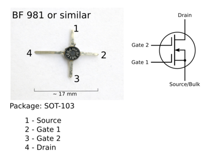
Representation of a dual-gate MOSFET BF981 (or similar type). In the circuit symbol, the protective diodes on the gates have been left out.
.svg)

Advantages and disadvantages
A fundamental disadvantage of MOSFET technology is the low surface mobility of the charge carriers in the channel. Electrons have a higher mobility than defect electrons, which is why n-channel MOSFETs have better properties than p-channel types. However, by making the component structures smaller, this disadvantage can be compensated for and the switching speed is increased. This makes it possible, on the one hand, to produce faster individual transistors, on the other hand, thanks to fine honeycomb structures, fast MOSFETs for large currents can also be produced. By scaling into the submicrometer range, the MOSFET can be used for integrated digital applications with clock frequencies above 1 GHz. Because of their simple manufacturing process (CMOS process) and the lateral structure, MOSFETs are particularly suitable for integrated circuits .
Since IGFETs, in contrast to bipolar transistors, are not controlled by a current flow (base current) but by a control voltage, they are misleadingly referred to as "de-energized". In static operation, i.e. i.e., with a constant gate voltage, there is almost no current flowing through the gate. However, a sometimes considerable charge and discharge current is necessary to charge the gate capacitance. Together with the gate leakage currents, which are no longer negligible in today's microprocessors, these currents cause the high power consumption of modern integrated circuits.
In power applications is power MOSFET in terms short switching times and low switching losses of the bipolar transistors and IGBTs superior. However, it does not reach their high blocking voltages. Compared to bipolar technology, the drain-source path of the MOSFET has a pure resistance characteristic which determines the static voltage drop and the static power loss during operation. Only then are the high efficiencies of power electronic circuits possible, especially at low voltages and battery operation (see synchronous rectifier ).
In contrast to bipolar transistors, the channel resistance of the drain-source path of the MOSFET has a positive temperature coefficient. This means that when the temperature rises, so does the resistance. As a result, several MOSFETs can often be connected in parallel for pure switching applications without additional symmetrizing measures in order to increase the current carrying capacity and reduce the voltage drop. As soon as one of the MOSFETs gets too hot due to too much current, its resistance increases. As a result, differences in current distribution in MOSFETs are reduced instead of increasing as is the case with polar transistors.
Silicon-based power MOSFETs are advantageously used for switching voltages of up to 800 V and currents of up to several hundred amperes. Areas of application include a. Switching power supplies, synchronous rectifiers, clocked current and voltage regulators and also powerful high-frequency transmitters up to the VHF range. In special applications, switching times of just a few nanoseconds at voltages of several kilovolts are achieved by connecting them in series.
handling
MOSFETs have very high resistance by the insulation of the gate compared to the source-drain channel, a great sensitivity to electrostatic discharges (engl. Electro-static discharge , ESD ) on. In the event of improper handling of electronic components that consist of field effect transistors, this leads to a breakdown of the gate insulating layer and thus to the destruction of the field effect transistors. The resulting difficulties in handling were one of the reasons why field effect transistors were only able to establish themselves on the market a few decades later compared to bipolar transistors . In many cases, protective wire bridges between gate and source (drain, bulk) could only be removed after the MOSFET was soldered into the application circuit. In principle, however, power MOSFETs are sufficient due to their lying mostly in Nanofaradbereich gate capacitance electrostatic charging of course are usually no longer needed here - such as external jumpers - protected so that special protective measures. Today's discrete low-power field effect transistors and integrated circuits also usually have integrated protective diodes with resistors or corresponding semiconductor structures on the connection lines, which minimize the effects of electrostatic discharges on the sensitive gate insulating layer. Nevertheless, when handling field effect transistors, special precautionary measures must still be taken to avoid electrostatic charges. For example, work and production areas in which field effect transistors are used are marked with ESD warning signs. In addition, the manufacturer's information must always be observed.
See also
literature
- Hans-Joachim Fischer, Wolfgang E. Schlegel: transistor and circuit technology . 4th edition. Military publishing house of the GDR, Berlin 1988.
- Hans-Günther Wagemann, Tim Schönauer: silicon planar technology. Basic processes, physics and components . Teubner, Stuttgart / Leipzig / Wiesbaden 2003, ISBN 3-519-00467-4 .
Web links
- Java applet for NMOS
- Electronics Compendium - MOS Field Effect Transistor (MOS-FET)
- Computer History Museum: [1] . On: computerhistory.org.
Individual evidence
- ↑ Patent US1745175 : Method and Apparatus For Controlling Electric Currents. Inventor: JE Lilienfeld ( PDF ).
- ↑ Sami Franssila: Introduction to Microfabrication . John Wiley and Sons, 2010, ISBN 978-0-470-74983-8 , pp. 229 .
- ↑ a b Yaduvir Singh, Swarajya Agnihotri: Semiconductor Devices . IK International Pvt Ltd, 2009, ISBN 978-93-8002612-1 , pp. 128-130 .
- ↑ Microwave Encyclopedia, Micorowaves101.com: LDMOS , accessed Nov. 29, 2008
- ↑ cf. Michael Reisch: Semiconductor components . Springer, 2007, ISBN 978-3-540-73200-6 , pp. 219 ( limited preview in Google Book search).
- ↑ Ulrich Tietze, Ch. Schenk: Semiconductor circuit technology . 12th edition. Springer, 2002, ISBN 3-540-42849-6 , pp. 204 .
- ↑ Michael Reisch: Semiconductor components . Springer, 2007, ISBN 978-3-540-73199-3 , pp. 226 .
- ↑ Kurt Hoffmann: System integration: from transistor to large-scale integrated circuit . 2nd, corrected and advanced Edition Oldenbourg, Munich [u. a.] 2006, ISBN 3-486-57894-4 , 4.5.2 channel length modulation, p. 188-190 .
- ↑ Carl Walding: Not only losses minimized ( page no longer available , search in web archives ) Info: The link was automatically marked as defective. Please check the link according to the instructions and then remove this notice. . elektroniknet.de. Retrieved September 20, 2008.
- ↑ Martin Stiftinger: Simulation and modeling of high-voltage DMOS transistors . Dissertation, Vienna University of Technology, 1994.
- ^ Gordon Moore: No Exponential is Forever ... but We Can Delay 'Forever'. International Solid State Circuits Conference (ISSCC), USA, 2003
- ↑ YS Borkar: VLSI Design Challenges for Gigascale Integration. '18th Conference on VLSI Design, Kolkata, India, 2005
- ↑ ITRS - International Technology Roadmap for Semiconductors 2006 Update. Technical report, 2006
- ↑ Xuejue Huang et al. a .: Sub 50-nm FinFET: PMOS . In: Electron Devices Meeting, 1999. IEDM Technical Digest. International . 1999, p. 67-70 , doi : 10.1109 / IEDM.1999.823848 .
- ↑ D. Hisamoto, WC Lee, J. Kedzierski, H. Takeuchi, K. Asano, C. Kuo, E. Anderson, TJ King, J. Bokor, C. Hu: FinFET-a self-aligned double-gate MOSFET scalable to 20 nm . In: Electron Devices, IEEE Transactions on . tape 47 , no. 12 , 2000, pp. 2320-2325 , doi : 10.1109 / 16.887014 ( PDF ).
- ^ EJ Nowak, I. Aller, T. Ludwig, K. Kim, RV Joshi, Ching-Te Chuang, K. Bernstein, R. Puri: Turning silicon on its edge - double gate CMOS / FinFET technology . In: IEEE Circuits and Devices Magazine . tape 20 , no. 1 , 2004, p. 20-31 , doi : 10.1109 / MCD.2004.1263404 .
- ↑ FinFET monopoly broken - FinFETs for everyone. Retrieved January 4, 2014 .