Rise and fall time

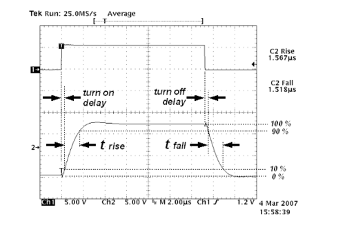
Under rise time and fall time (English rise time and fall time ) is understood in the digital technology and measurement technology the time a level change of an (ideally) rectangular signal requires real to its signal level between two defined intermediate values are (usually 10% and 90% ) to change.
The times are caused by the finite limit frequency of the switching elements and transmission paths involved.
Digital technology
In digital technology and with switching transistors, rise and fall times describe the times during which the signal no longer has the old and not yet the new defined logic level ("0" or "1") or switching state. See also slope .
In digital technology which in the worst case (here mostly are worst case ) called guaranteed times. They describe the time that a signal (for example in a computer processor ) needs to safely switch between the two binary states. The rise and fall times specified for a component are often not measured values , but rather minimum values assured for certain parameters ( operating voltage , temperature) by the design and manufacturing process of the component or the logic family under consideration .
All digital technology is based on circuit elements that are optimized for processing digital signals, but ultimately work analog . It should be noted that the assignment of “1” or “0” to “ current on ” or “current 0” is an idealization - in practice, however, voltage and current levels are normally used that deviate from these ideal values . Furthermore, the behavior of the circuit when the state changes is mostly asymmetrical, which is why the rise and fall times then differ to a greater or lesser extent.
Because of the non-ideal properties described, it is necessary to define threshold values for a logic signal. For logic "0", for example, a permissible range of 0 ... 0.8 V is specified for TTL and a range of 2 ... 5 V for logic "1". The actual switching threshold of the logic modules is in the "forbidden area" between these two values ( typically around 1.4 V); it is therefore exceeded during the rise and fall times. For digital circuits (logic modules) to function correctly, it is necessary to pass through the prohibited area with sufficient speed; A minimum permissible voltage rise rate or maximum rise / fall time is then specified accordingly .
Rise and fall times describe the time intervals in which this undefined “forbidden” state occurs during the switchover. This is particularly important for edge- triggered circuits, i.e. H. Circuits that react to the change in the signal (e.g. edge - triggered flip - flop ). Otherwise, it may cause malfunction ; see race condition . For example, for a flip-flop (SN74HC74) manufactured using HCMOS technology, a maximum value of 500 ns (operation with 4.5 V) is specified.
In order to maintain security against interference, the requirements for the outputs of these modules are more stringent than for the inputs. For example, a gate output in classic TTL technology is max. 0.4 V for "0" and min. 2.4 V guaranteed for “1”.
Very short rise and fall times in the signal also mean that there are very high frequency components in the spectrum of the signal that lead to the emission (radiation) of electromagnetic waves . Other circuit parts can be influenced in their function by these interfering signals . In order to ensure electromagnetic compatibility , the outputs of digital and driver circuits are designed so that the rise and fall times are only as short as absolutely necessary. For this purpose, the slew rate of the output driver is limited.
measuring technology
In measurement technology and for the characterization of analog and digital circuits , the values of 10% or 90% of the switching level or target signal are usually defined to specify the times.
Also switching transistors and other power electronic components are characterized with it.
Analog amplifiers, switching amplifiers , light emitting diodes , lasers , photodiodes and phototransistors are also characterized by rise and fall times that they provide in response to a step function .
If an exponential curve is assumed, the rise and fall times for a first- order low-pass filter or comparable systems are:
With
- the time constant
- the 3 dB cutoff frequency .
This formula is mostly derived from first-order filters. In higher order systems the error is quite small; For example, with higher-order low-pass filters, the rise time can be calculated relatively precisely from the 3 dB cutoff frequency; the most common overshoot has relatively little influence on this.
Additional delay times are characteristic of digital circuits as well as amplifiers, sensors and actuators (English delay times , for switching stages turn-on delay and turn-off delay ). These pass until the output voltage begins to change after a jump in the input signal, i.e. H. before the actual rise or fall time begins and depend on further poles and zeros of the transfer function or on non-linear memory effects .
The total time delay when a signal passes through a switching stage or another quadrupole thus results from the delay and approximately half the rise or fall time.
Many digital storage oscilloscopes have measurement functions for the delay as well as the rise and fall times.
See also
Individual evidence
- ↑ Data sheet from Texas Instruments : SNx4HC74 Dual D-Type Positive-Edge-Triggered Flip-Flops With Clear and Preset , "SCLS094E", December 1982, revised in December 2015


