
Intel Haswell microarchitecture
| Haswell (micro architecture) | |
|---|---|
| Manufacturer | Intel |
| Manufacturing process | 22 nm |
| base | Socket 1150 rPGA 947 BGA 1364 BGA 1168 |
| Sales description |
Core i3, 4th generation Core i5, 4th generation Core i7, 4th generation Xeon Celeron Pentium |
| Cores / threads | 2–4 (Desktop) 6+ (Extreme) 8+ (Xeon) |
| L1 cache | 32 + 32 kB per core |
| L2 cache | 256 kB per core |
| L3 cache | 2–8 MB (shared) |
| L4 cache | N / A or 128 MB (Iris Pro models) |
| predecessor | Sandy Bridge (tock) Ivy Bridge (tick) |
| successor | Broadwell (tick) Skylake (tock) |

Haswell is the code name of a processor micro- architecture from the chip manufacturer Intel , which appeared as the successor to the Ivy Bridge architecture in the 2nd quarter of 2013. Like Ivy Bridge, Haswell is also based on the 22 nm process. The integrated GPU also supports DirectX 11.1 and OpenGL 4.0. Mainboards with socket 1150 and one of the new 80s chipsets are required. For the Haswell processors of the second generation, also called Haswell Refresh, the chipsets of the 90 series are intended.
The Haswell processors were officially presented on June 1, 2013, a few days before the start of the Computex IT trade fair . However, individual dealers in China and other parts of Asia began selling Haswell processors and LGA1150 mainboards earlier.
The code name was derived from the town of Haswell in the US state of Colorado .
design
Haswell has been specially optimized for energy efficiency and performance in order to take advantage of the new FinFET transistors that were introduced when switching to the 22 nm manufacturing process.
Chipset for Haswell processors
Haswell processors are not compatible with the chipsets for the Ivy Bridge processors. In addition, Intel and Haswell are introducing new chipsets with additional features, such as more USB 3.0 interfaces.
Explanations

- ULT = Ultra Low Thermal Design Power ; ULX = Ultra Low eXtreme TDP.
- Only certain BGA versions will have a GT3 (Intel HD 5000, Intel Iris 5100) or GT3e (Intel Iris Pro 5200) integrated graphics unit. All other models receive the GT2 (Intel HD 4X00) integrated graphics unit. For more information, see Intel HD Graphics .
- Since ultrabooks and tablets require low energy consumption, Haswell ULT and Haswell ULX processors will only be available in a dual-core version. All other versions are dual or quad core models.
power
Compared to Ivy Bridge , Haswell has approximately 8% more vector processing power and up to 6% better single-thread performance. In addition, a Haswell processor consumes approx. 8% less power under load than a comparable Ivy Bridge model. In addition, an improvement in sequential CPU performance of 6% compared to Ivy Bridge can be recorded (instead of 6 now 8 execution ports per core). The main optimization was carried out with the integrated graphics unit, which achieved a 20% increase in performance compared to the predecessor Intel HD 4000 (Haswell HD 4600 vs. Ivy Bridge HD 4000).
Models
Haswell appeared in several versions:
Haswell-DT
Desktop version (socket LGA1150 )
- Quad-core processor
- L1 cache: 32 + 32 KiB per core (data + instructions)
- L2 cache: 256 KiB per core with processor clock
- L3 cache: 2 MiB to 8 MiB
- MMX , SSE , SSE2 , SSE3 , SSSE3 , SSE4 .2, Intel 64 , EIST , XD-Bit , IVT , AES instructions, AVX , AVX2 , SMT , TXT , gather, BMI1 , BMI2 , FMA3
- integrated GPU
- Socket 1150
- Power dissipation ( TDP ): 35-84 W.
- Release DATE: June 4, 2013
- Manufacturing technology: 22 nm
- The size: 177 mm² with 1.4 billion transistors (incl. IGPU and integrated Northbridge)
- Clock rates: 2.3–4.4 GHz
- Models : Intel Core i7-4770 series
Haswell MB
Mobile version ( PGA socket)
Haswell ( BGA version)
- 47 W and 57 W TDP : Haswell-H (for "all-in-one" systems, mini-ITX mainboards and other mainboards in a small form factor)
- 13.5 W and 15 W TDP ( MCM ): Haswell ULT (for Intel's ultrabook platform)
- 10 W TDP ( SoC ): Haswell-ULX (for tablet computers and certain ultrabook implementations)
Haswell-E
High-end desktop (FCLGA2011-3)
- Six-core processor (hexa-core) / eight-core processor (octa-core) # * L1 cache: each core 32 + 32 KiB (data + instructions)
- L2 cache: 256 KiB per core with processor clock
- L3 cache: 15 MiB to 20 MiB
- MMX , SSE , SSE2 , SSE3 , SSSE3 , SSE4 .2, Intel 64 , EIST , XD-Bit , IVT , AES instructions, AVX , AVX2 , SMT , TXT , gather, BMI1 , BMI2 , FMA3
- Base 2011-3
- Power dissipation ( TDP ): 140 W
- Release DATE: August 29, 2014
- Manufacturing technology: 22 nm
- The size: 356 mm² with 2.6 billion transistors (including integr. Northbridge)
- Clock rates: 3.0-3.7 GHz
- Models : Intel Core i7-5900 series
Haswell EP
Server version (FCLGA2011-3)
Roadmap
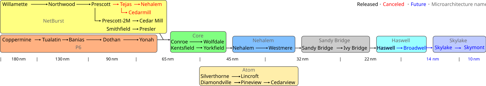
Intel CPU Core project plans from the NetBurst or P6 to Skylake

See also
Web links
- Golem article on Haswell micro-architecture
- Desktop 4th Generation Intel Core Processor Family, Desktop Intel Pentium Processor Family, and Desktop Celeron Processor Family. (PDF) Intel, October 2015, accessed on January 12, 2016 (English, errata with a list of known errors in the Haswell micro-architecture).
Individual evidence
- ↑ Haswell processors already available in China . In: computerbase.de , accessed on May 12, 2013.
- ^ Andy Vuong: Intel's newest processor named after small Colorado town of Haswell. In: The Denver Post. Digital First Media, February 6, 2013, accessed July 17, 2014 .
- ↑ Ryan Shrout: IDF 2012: Intel Haswell Architecture Revealed. In: PC Perspective. Retrieved September 22, 2013 .
- ↑ IDF: Intel says Haswell won't use Ivy Bridge transistors . In: The Inquirer
- ↑ a b c d Gennadiy Shvets: Intel Core i5-3570K vs i5-4670K . July 9, 2013. Retrieved July 23, 2013.
- ↑ xbitlabs.com
- ↑ pcpro.co.uk
- ↑ bit-tech.net
- ↑ Intel Haswell and Broadwell Silicon Variants Detailed . In: techPowerUp
- ↑ The new Intel Haswell-EP (Server Mile Technet)
x86 microarchitectures: 8086 | 80186 | 80286 | 80386 | 80486 | P5 | P6 | NetBurst | Core Solo / Core Duo | Core 2 | Nehalem / Westmere | Sandy Bridge / Ivy Bridge | Haswell | Broadwell | Skylake | Kaby Lake | Coffee Lake | Whiskey Lake | Cannon Lake | Cascade Lake | Ice Lake | Comet Lake | atom
Non-x86 microarchitectures: Microcontrollers: MCS-48 | MCS-51 | MCS-96 | XScale • Server: Itanium | Itanium 2
GPU microarchitectures: Larrabee | Intel HD Graphics