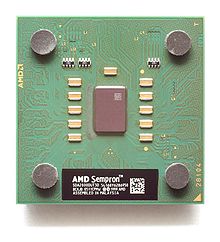
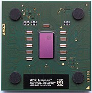
AMD Sempron (K7)
| << AMD Sempron >> | |
|---|---|
 AMD Sempron emblem |
|
| Production: | 2004 to 2005 |
| Producer: | AMD |
| Processor clock: | 1.5 GHz to 2.2 GHz |
| FSB cycle: | 166 MHz to 200 MHz |
| L2 cache size: | 256 KiB to 512 KiB |
| Instruction set : | x86 |
| Microarchitecture : | K7 |
| Base: | Base A |
Names of the processor cores:
|
|
With the AMD Sempron based on the K7 architecture , AMD continued the path started with the AMD Duron in 2004 to offer processors in the low-price segment under its own brand name. At the same time, new AMD Sempron processors based on the K8 architecture were presented, which over time replaced Semprons based on the K7 architecture.
Technical
The AMD Semprons have a lower clocked front side bus and are usually only available with lower clock frequencies than the corresponding AMD Athlon XPs . This limits the performance of these CPUs, but the lower production costs also reduce the sales price.
The processor cores are identical to the cores of the faster Athlon XP processors.
Model data socket A
Thoroughbred B
- L1 cache: 64 + 64 KiB (data + instructions)
- L2 cache: 256 KiB with processor clock
- MMX , 3DNow! , SSE
- Socket A , EV6 with 166 MHz (FSB 333)
- Operating voltage (VCore): 1.60 V.
- Power consumption ( TDP ): 62 W
- First release date: July 28, 2004
- Manufacturing technology: 130 nm
- The size: 84.66 mm² with 37.2 million transistors
- Clock rates: 1,500–2,000 MHz
- 2200+: 1,500 MHz
- 2300+: 1,583 MHz
- 2400+: 1,667 MHz
- 2500+: 1,750 MHz
- 2600+: 1,833 MHz
- 2800+: 2,000 MHz
Thorton
- L1 cache: 64 + 64 KiB (data + instructions)
- L2 cache: 256 KiB with processor clock
- MMX , 3DNow! , SSE
- Socket A , EV6 with 166 MHz (FSB 333)
- Operating voltage (VCore): 1.60 V.
- Power consumption ( TDP ): 62 W
- First release date:
- Manufacturing technology: 130 nm
- The size: 100.99 mm² with 54.3 million transistors
- Clock rates: 1,500–2,000 MHz
- 2200+: 1,500 MHz
- 2400+: 1,667 MHz
- 2800+: 2,000 MHz
Barton
- L1 cache: 64 + 64 KiB (data + instructions)
- L2 cache: 512 KiB with processor clock
- MMX , 3DNow! , SSE
- Socket A , EV6 with 166 (FSB 333) or 200 MHz (FSB 400)
- Operating voltage (VCore): 1.60 V.
- Power consumption ( TDP ): 62 W
- First release date: September 17, 2004
- Manufacturing technology: 130 nm
- The size: 100.99 mm² with 54.3 million transistors
- Clock rates: 2,000 - 2,200 MHz
- 3000+: 2,000 MHz (166 MHz FSB)
- 3300+: 2,200 MHz (200 MHz FSB)


