AMD Am486
| << AMD Am486 >> | |
|---|---|
| Production: | since 90s |
| Producer: | AMD |
| Processor clock: | 25 MHz to 120 MHz |
| FSB cycle: | 25 MHz to 50 MHz |
| L1 cache size: | 8 kB to 16 kB |
| Instruction set : | x86 |
| Base: | Base 3 |

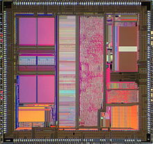
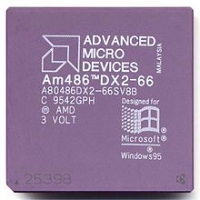
The Am486 processor family is AMD's counterpart to the i486 processor family from Intel.
history
In the early 1990s, there were (still) far-reaching agreements between Intel and AMD for the exchange of technology. Therefore the 486 CPUs of both families initially differ only insignificantly. The microcode of the early AMD variants still corresponded to that of the Intel models, which is why 486 CPUs from Intel and AMD did not show any practical differences at that time.
However , AMD was not allowed to adopt the microcode of the Intel DX4 , which was modified due to technical changes to the CPU core and bus interface - often also called i486DX4 , although Intel never called it that - which is why the Am486DX4 was developed from the Am486DX2 on its own by AMD. The performance of the Am486DX4 initially lagged behind those of the DX4 from Intel, which was equipped with larger L1 caches , an improved multiplication unit and later also with an improved L2 cache controller.
AMD later developed the Am486DX4 into the Enhanced Am486DX4 and the Am5x86 . Both are fast 486 CPUs, with which AMD made up for some technical improvements that Intel had already made with the first Intel DX4 . For example, the Am5x86-PR75 with its core clock of 133 MHz was on par with a Pentium 75, as the name component “PR75” (the “PR” stands for Pentium Rating ) tries to suggest .
Model data Am486
Am486DX
Comparable to the Intel i486DX
Technical specifications
- L1 cache: 8 kB
- L2 cache: depending on the mainboard or chipset used
- Socket 3 with an FSB of 25, 33 or 40 MHz
- Operating voltage (VCore): 5 V
- Release DATE: 1993
- Manufacturing technology: 0.7 µm
- The size:? mm² at? Million transistors
- Clock rates: 25, 33 and 40 MHz
Am486DE2
CPU for embedded applications with clock doubling.
Technical specifications
- L1 cache: 8 kB (write through)
- Operating voltage: 3V VCore and 5V I / O
- Manufacturing engineering: ?
- Power management, two-pin system management interrupt (SMI)
- Clock rates: 66 MHz
- Package: 208-lead SQFP or 168-pin PGA
Am486SX
Corresponds to the Am486DX but without an integrated coprocessor. Comparable to the Intel i486SX
Technical specifications
- L1 cache: 8 kB
- L2 cache: depending on the mainboard or chipset used
- Socket 3 with an FSB of 25, 33 or 40 MHz
- Operating voltage (VCore): 5 V
- Publication date:
- Manufacturing technology: 0.7 µm
- The size:? mm² at? Million transistors
- Clock rates: 33 and 40 MHz
Am486DX2
Corresponds to the Am486DX , but with internal clock doubling. Comparable to the i486DX2
Technical specifications
- L1 cache: 8 kB
- L2 cache: depending on the mainboard or chipset used
- Socket 3 with an FSB of 25, 33 or 40 MHz
- Operating voltage (VCore): 5 V (0.7 µm), later 3.3 V (0.5 µm)
- Publication date:
- Manufacturing technology: 0.7 µm, later 0.5 µm
- The size:? mm² at? Million transistors
- Clock rates: 50 MHz (0.7 µm version only), 66 and 80 MHz
Am486SX2
Corresponds to the Am486SX , but with internal clock doubling. Comparable to the Intel i486SX2
Technical specifications
- L1 cache: 8 kB
- L2 cache: depending on the mainboard or chipset used
- Socket 3 with an FSB of 25 or 33 MHz
- Operating voltage (VCore): 5 V
- Publication date:
- Manufacturing technology: 0.7 µm
- The size:? mm² at? Million transistors
- Clock rates: 50 and 66 MHz
Am486DX4
Corresponds to the Am486DX , but with internal clock tripling . Comparable to the Intel DX4 , but only with 8 kB instead of 16 kB L1 cache.
Technical specifications
- L1 cache: 8 kB
- L2 cache: depending on the mainboard or chipset used
- Socket 3 with an FSB of 25, 33 or 40 MHz
- Operating voltage (VCore): 3.3V
- Publication date:
- Manufacturing technology: 0.5 µm
- The size:? mm² at? Million transistors
- Clock rates: 75, 90 ( OEM ), 100 and 120 MHz
Model data Enhanced Am486
The Enhanced Am486 supports extended power-saving modes and the write-back method for the L1 cache. At first it was only available with 8 kB, later also with 16 kB L1 cache.
Enhanced Am486DX2
Improved variant of the Am486DX2 : initially 8, later also 16 kB write-back L1 cache
Technical specifications
- L1 cache: 8 or 16 kB
- L2 cache: depending on the mainboard or chipset used
- Socket 3 with an FSB of 25, 33 or 40 MHz
- Operating voltage (VCore): 3.30 or 3.45 V.
- Publication date:
- Manufacturing technology: 0.50 µm (8 kB L1 cache); 0.35 µm (16 kB L1 cache)
- The size:? mm² at? Million transistors
- Clock rates:
- 8 kB L1 cache: 66 and 80 MHz
- 16 kB L1 cache: 66 MHz
Enhanced Am486DX4
Improved variant of the Am486DX4 : initially 8, later also 16 kB write-back L1 cache
Technical specifications
- L1 cache: 8 or 16 kB
- L2 cache: depending on the mainboard or chipset used
- Socket 3 with an FSB of 25, 33 or 40 MHz
- Operating voltage (VCore): 3.30 or 3.45 V.
- Publication date:
- Manufacturing technology: 0.50 µm (8 kB L1 cache); 0.35 µm (16 kB L1 cache)
- The size:? mm² at? Million transistors
- Clock rates:
- 8 kB L1 cache: 75, 100 and 120 MHz
- 16 kB L1 cache: 100 and 120 MHz
Am5x86 (X5)
Based on the Enhanced Am486DX4 with 16 kB L1 cache. Because of the high clock frequency, the internal clock quadrupling and for marketing reasons it was sold as a 5x86. See Am5x86 for technical details etc.
See also
Web links
Data Sheets
- Enhanced Am486 Microprocessor Family (PDF file; 1.5 MB)
- Am486DE2 (PDF file; 1.2 MB)
- AMD Am486 info page ( Memento from February 25, 2008 in the Internet Archive )
- Am486DX / DX2 (PDF file; 4.7 MB)
- Am486DX2 Low-Voltage (PDF file; 452 kB)
- Am486DX4 (PDF file; 365 kB)


