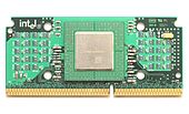
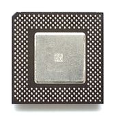
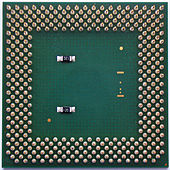
Intel Celeron (P6)
| Intel Celeron >> | |
|---|---|
 Celeron emblem |
|
| Production: | 1998 to 2002 |
| Producer: | Intel |
| Processor clock: | 266 MHz to 1.4 GHz |
| FSB cycle: | 66 MHz to 100 MHz |
| L2 cache size: | 0 KiB to 256 KiB |
| Instruction set : | x86 |
| Microarchitecture : | Intel P6 |
| Base: | |
Names of the processor cores:
|
|
The Intel Celeron processors based on the Intel P6 architecture were the first processors developed specifically for the low-price segment. With them, Intel introduced the brand name Intel Celeron . With the introduction of the NetBurst architecture in 2002, these processors were replaced by Intel Celerons based on this architecture .
Technical
The first models of the Intel Celeron come from the Pentium II , later models of the P6 microarchitecture from the Pentium III .
The first Celeron (Covington) with clock rates from 266 MHz came onto the market without any L2 cache , which led to a paradoxical situation that is still technically valid: Without this L2 cache, the Covington is not only considerably slower than a Pentium II, it even has to admit defeat to a first-generation Pentium clocked at only 200 MHz in many areas of application . In contrast, the performance of a Pentium II clocked at 233 MHz is in some cases considerably higher than that of a Pentium clocked at 200 MHz.
Then Intel equipped the Celeron with a 128 KiB L2 cache, which - in contrast to that of the Pentium II - is not only operated at half but at the full CPU clock frequency. The Celeron has a smaller, but twice as fast cache. Therefore, the second Celeron generation (Mendocino) is even faster than a Pentium II with the same clock in some areas of application.
Interestingly enough, Covington still had buyers: At that time, attempts to overclock did not usually fail on the processor core itself, but on its L2 cache, which was often unable to cope with the higher clock frequencies. Since the Covington does not have an L2 cache, however, the processor can sometimes be operated with significantly higher clock frequencies.
The Mendocino-Celeron can also be overclocked quite well: The Celeron 300A (the suffix “A” is only used to differentiate it from the 300 MHz Covington) can often be cooled with 450 MHz at an FSB clock frequency of 100 MHz the intended 66 MHz. In order to achieve this, the slot 1 pin B21 can be masked or isolated in order to trick the motherboard into thinking that a Pentium II with 100 MHz FSB clock is installed.
On motherboards for the Pentium II, which only support 66 MHz FSB clock, a noticeable increase in performance is achieved by replacing the Pentium II clocked at a maximum of 333 MHz with a Mendocino-Celeron clocked at 500 MHz or 533 MHz the low-priced particular processor becomes an upgrade processor. An adapter from socket 370 to slot 1 is required for this exchange, although no further requirements are placed on this adapter in this case.
Model data slot 1
Covington
- L1 cache: 16 + 16 KiB (data + instructions)
- L2 cache: nonexistent
- MMX
- Slot 1 , GTL + with 66 MHz FSB
- Power dissipation ( TDP ):
- Operating voltage ( VCore ): 2.0V
- Release DATE: April 15, 1998
- Manufacturing technology: 250 nm
- The size: 118 mm² with 7.5 million transistors
- Clock rates:
- 266 MHz
- 300 MHz
Mendocino
- L1 cache: 16 + 16 KiB (data + instructions)
- L2 cache: 128 KiB with processor clock
- MMX
- Slot 1 , GTL + with 66 MHz FSB
- Operating voltage ( VCore ): 2.0V
- Power dissipation ( TDP ):
- Release DATE: Aug. 24, 1998
- Manufacturing technology: 250 nm
- The size: 154 mm² with 19.2 million transistors
- Clock rates:
- 300 MHz
- 333 MHz
- 366 MHz
- 400 MHz
- 433 MHz
Model data base 370
Mendocino
- L1 cache: 16 + 16 KiB (data + instructions)
- L2 cache: 128 KiB with processor clock
- MMX
- Socket 370 PPGA, GTL + with 66 MHz FSB
- Core Voltage (VCore): 2.0V
- Power Dissipation ( TDP ): 17.8-28.3 W.
- Release DATE: 1999
- Manufacturing technology: 250 nm
- The size: 154 mm² with 19.2 million transistors
- Clock rates: 300 to 533 MHz
- 300 MHz
- 333 MHz
- 366 MHz
- 400 MHz
- 433 MHz
- 466 MHz
- 500 MHz
- 533 MHz
Coppermine-128
- L1 cache: 16 + 16 KiB (data + instructions)
- L2 cache: 128 KiB with processor clock
- MMX , SSE
- Socket 370 FC-PGA, GTL + with 66 or 100 MHz FSB
- Core voltage (VCore): 1.50-1.75V
- Power dissipation ( TDP ): 11.2-32.0 W.
- Release DATE: March 29, 2000
- Manufacturing technology: 180 nm
- The size: 106 mm² with 28.1 million transistors
- Clock rates:
- 66 MHz FSB
- 533 MHz
- 566 MHz
- 600 MHz
- 633 MHz
- 666 MHz
- 700 MHz
- 733 MHz
- 766 MHz
- 100 MHz FSB
- 800 MHz
- 850 MHz
- 900 MHz
- 950 MHz
- 1000 MHz
- 1100 MHz
- 66 MHz FSB
Tualatin-256
- L1 cache: 16 + 16 KiB (data + instructions)
- L2 cache: 256 KiB with processor clock
- MMX , SSE
- Socket 370 FC-PGA2, AGTL with 100 MHz FSB
- Core voltage (VCore): 1.475-1.50V
- Power Dissipation ( TDP ): 28.9-34.8 W.
- Release DATE: October 2, 2001
- Manufacturing technology: 130 nm
- The size: 80 mm² with 44 million transistors
- Clock rates:
- 900 MHz
- 1000 MHz
- 1100 MHz
- 1200 MHz
- 1300 MHz
- 1400 MHz
Individual evidence
- ↑ Tom's Hardware: How to Get All 66 MHz Slot 1 CPUs Running 100 MHz , article from May 14, 1998
Web links
- Intel Pentium II - and Pentium III -Celerons on cpu-collection.de


