Intel i486
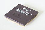
The Intel 80486 or i486 microprocessor was developed by Intel as the successor to the i386 and was the first CPU of the 80486 generation on the market. The 486 (pronounced "eighty-six"), as the 80486 is often called, was manufactured under license by Intel's competitor AMD and sold as the Am486 . The clock frequencies of the i486 were 16 MHz (i486SX) to 100 MHz (DX4). As a successor, the manufacturer Intel developed the Pentium processor.
The 486 generation was released in 1989 and dominated the PC market from around 1992 to 1995. At first, the computers equipped with the 486 were very expensive and cost the equivalent of around 6,000 euros and more. They were therefore not or hardly affordable for normal users until around 1992. The 80486 is a processor, which in its first prototype still manages without active cooling and with suitably dimensioned housing ventilation even without a passive heat sink (80486DX33). A typical system this time had as a 120- MB - HDD , 4 MiB main memory , a VGA graphics card and operating system MS-DOS 5.0 with Windows 3.1 as a graphical user interface.
Significant changes compared to the predecessor i386 were the integrated (L1) cache and the integrated floating point arithmetic unit (sometimes switched off again in later SX versions).
General models
The 80486 itself does not have an L2 cache, the L2 cache is located on the mainboard like the 80386 . The size of the L2 cache and its parameters depend on the mainboard , the chipset used and the actual cache configuration (DIL sockets into which 5 or 9 sRAM modules were to be plugged were common). 32, 64, 128, 256 or rarely 512 KByte L2 cache were common.
i486DX
- Code name: P4
- L1 cache: 8 KiB
- Socket 486 , socket 1 , socket 2 , socket 3 with a front side bus of 16, 25, 33 or 50 MHz
- Operating voltage ( VCore ): 5 V
- Release DATE: 1989
- Manufacturing technology: CHMOS IV with 1.0 µm
- Housing: CPGA -168, TQFP-176 and PQFP-196
- The size: 81 mm² with 1.2 million transistors
- Clock frequencies: 25, 33 or 50 MHz
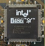
i486SX
The i486SX is an i486 with or without a switched off FPU . In this way, Intel was able to sell processors with defective floating point units as an inexpensive alternative instead of having to dispose of them.
- Code name: P4S / P23
- L1 cache: 8 KiB
- Socket 486 , socket 1 , socket 2 , socket 3 with a front side bus of 16, 20, 25 or 33 MHz
- Operating voltage ( VCore ): 5 V
- Release DATE: September 1991
- Manufacturing technology: CHMOS IV with 1.0 µm
- The size: 66 mm² with 1.185 million transistors
- Housing: CPGA-168, TQFP-176, PQFP -132, PQFP-196 and PQFP-208
- Clock frequencies: 16, 20, 25 or 33 MHz
i486DX2
The DX2 in the name refers to the doubling of the internal CPU clock compared to the clock of the front side bus. A DX2 / 66 had an internal clock frequency of 66 MHz with an external clock frequency of 33 MHz.
- L1 cache: 8 KiB ( write-through , write-back )
- Socket 486 , socket 1 , socket 2 , socket 3 with a front side bus of 20, 25 or 33 MHz
- Operating voltage ( VCore ): 5V, 3.3V
- Release DATE: March 1992
- Manufacturing technology: CHMOS V with 0.8 µm
- Die size: 76 mm² with 1.2 million transistors (weight: approx. 24 g)
- Housing: CPGA-168, TQFP-176 and PQFP-208
- Clock frequencies: 40, 50 or 66 MHz
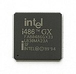
i486GXSF (FA80486GXSF33)
The i486GX is a processor for embedded applications. The CPU can be used in battery-operated devices thanks to its very low energy consumption. In terms of equipment, it roughly corresponds to an i486SX, apart from the external 16-bit data bus.
- L1 cache: 8 KiB ( write-through )
- Data bus: 16 bit
- Operating voltage ( VCore ): 2.0 V to 2.7 V.
- Operating voltage I / O: 3.3 V
- Publication date: ?
- Manufacturing engineering: ?
- The size: ? mm² at? Million transistors
- Housing: TQFP -176
- Clock frequencies:
- 0 MHz (stop clock mode, internal registers are designed as static RAM cells)
- 16 MHz from 2.0 V ( VCore )
- 20 MHz from 2.2 V (VCore)
- 25 MHz from 2.4 V (VCore)
- 33 MHz from 2.7 V (VCore)
i486SX2
- L1 cache: 8 KiB
- Socket 486 , socket 1 , socket 2 , socket 3 with a front side bus of 25 or 33 MHz
- Operating voltage ( VCore ): 5 V
- Publication date: ?
- Manufacturing engineering: ?
- The size:? mm² with 0.9 million transistors
- Housing: CPGA-168
- Clock frequencies: 50 or 66 MHz
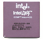
Intel DX4
The DX4 in the name refers to the tripling of the internal CPU clock compared to the front-side bus clock (an originally intended DX3 with a factor of 2.5 never came on the market). A DX4 / 100 had an internal clock frequency of 100 MHz with an external clock frequency of 33 MHz.
- L1 cache : 16 KiB ( write-through , write-back )
- Socket 3 with a front side bus of 25 and 33 MHz
- Operating voltage ( VCore ): 3.3V
- Release DATE: March 1994
- Manufacturing technology: 0.6 µm
- The size: 81 mm² with 1.6 million transistors
- Housing: CPGA-168 and SQFP-208
- Clock frequencies: 75 or 100 MHz
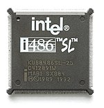
i486SL (-NM)
These energy-saving versions of the i486s were often used in entry-level notebooks that did not need a lot of power. Both processors can be described as the first notebook processors, as they were specially made for them. However, it was not until many years later that Intel presented a special notebook processor with the Pentium MMX Tillamook.
- L1 cache: 8 KiB
- FPU: yes, except i486SL-NM
- Socket 3 with a front side bus of 20, 25 or 33 MHz
- Operating voltage ( VCore ): 3.45 V.
- Release DATE: 1992
- Manufacturing engineering: ?
- Housing: PQFP-132
- Clock frequencies: 20, 25 or 33 MHz
Special models
i486 overdrive
An Intel i486 overdrive processor is intended for upgrading existing 80486 systems and is a special version of the respective i486DX2, i486SX2 and Intel DX4 processors.
In order for these overdrive processors to run in the older system environment, they have a predefined clock multiplication and ignore the external settings of the multiplier. In addition, they basically work with a 5 volt supply voltage. In the case of the overdrive version of the Intel DX4, there is a DC voltage converter on the processor surface , which generates the necessary processor operating voltage of 3.3 volts from the existing 5 volt supply.
The first OverDrive CPU is an i486DX2 presented in May 1992, which can be operated in an i486SX motherboard. This means that such a system can be retrofitted with an FPU that the i486SX lacks. The remaining variants of the i486 were then offered as OverDrive-CPU.
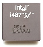
i487
The i487 (code name: P32S / P23N) was the math coprocessor ( FPU ) for the i486SX processors. However, the i487 was not a real coprocessor, but a full-fledged i486DX. The i487 deactivated the i486SX and took over all processor functions in the computer. To make this possible, the i487 has an additional pin compared to the i486DX. This pin also prevents the i487 from being used independently as a full-fledged i486DX.

