
Graph

Graphene [ gʁa'feːn ] (emphasis on the second syllable: Graph e n ; English graphene ) is the name for a modification of carbon with a two-dimensional structure, in which each carbon atom is surrounded by three more at an angle of 120 °, so that a forms a honeycomb pattern. Since carbon is tetravalent, there must be two double bonds per “honeycomb”, but these are not localized . It is a chain of benzene rings , as often occurs in aromatic compounds. Although a single benzene ring has three double bonds in the representation of the valence line formulas , connected benzene rings in this representation purely formally have only two double bonds per ring. Therefore, the structure can be better described by showing the delocalized bonds as a large circle in the benzene ring. The bond relationships in the graph are described in the graph structure . Graphene can be described as a polycyclic aromatic hydrocarbon . Other groups of atoms must be docked on the “edge” of the honeycomb lattice, but - depending on their size - they hardly change the properties of the graph.


In theory, single-layer carbon layers, graphenes, were first used to describe the structure and electronic properties of complex carbon materials.
Infinitely extended and flat, strictly two-dimensional structures are, however , not possible due to a rigorous mathematical theorem, the Mermin-Wagner theorem and its variants, as they are demonstrably thermodynamically unstable .
That is why there was general astonishment among chemists and physicists when Konstantin Novoselov , Andre Geim and their colleagues announced the representation of free, single-layer graphene crystals in 2004. Their unexpected stability could be explained by the existence of metastable states or by the formation of irregular waviness ( crumpling ) of the graphene layer.
In 2010 Geim and Novoselov were awarded the Nobel Prize in Physics for their research , after not only having made decisive contributions to the representation of these systems, but also having discovered many of their unusual properties.
The three-dimensional structure of graphite , with which graphene is structurally closely related, can be conceptually generated by stacking such single-layer layers . If, on the other hand, one imagines the single-layer layers rolled up, one obtains stretched carbon nanotubes . Likewise, some of the six rings can be replaced by rings of five, whereby the flat surface arches into a spherical surface and fullerenes result in certain numerical ratios : If, for example, 12 of 32 rings are replaced, the smallest fullerene is created (C 60 ). In theory, single-layer layers made from other tetravalent elements such as silicon and germanium are also possible. 2012 were in fact silicene layers demonstrated experimentally in the form of a gently undulating monolayer of silicon.
prehistory
Even before Geim and Novoselov people were concerned with graphs. In 1859, Benjamin Collins described Brodie Jr. the lamellar structure of thermally reduced graphite oxide . This was examined intensively in 1918 by Volkmar Kohlschütter and P. Haenni. They also reported on the production of graphite oxide paper . The first transmission electron microscope images (TEM images) of graphene with a low number of layers were published in 1948 by G. Ruess and F. Vogt. Hanns-Peter Boehm is one of the pioneers of graph research . As early as 1962 he reported on single-layer carbon foils and also coined the term graph.
In 1947, the theoretical physicist Philip Russell Wallace at McGill University in Montreal described the electrical properties of graphene, but experts doubted that 2D crystals like graphene could exist because they were too unstable.
structure
All carbon atoms in graphene are sp 2 - hybridized , which means that each carbon atom can form three equivalent σ-bonds to other carbon atoms. This results in a honeycomb structure known from the layers of graphite . The carbon-carbon bond lengths are all the same and are 142 pm . As in graphite, the third, non-hybridized 2p orbitals are perpendicular to the graphene plane and form a delocalized π bond system .
Graphene therefore consists of two equivalent sublattices A and B, to which the carbon atoms are assigned. The sublattices are shifted from one another by the length of the bond . The diatomic unit cell is spanned by the lattice vectors and . These point to the next but one neighbor. The length of the vectors and thus the lattice constant can be calculated


- .

Graphene can be understood as a single crystal on the one hand and as a huge molecule on the other . Smaller molecules such as B. benzene , hexabenzocoronen or naphthalene can be seen as hydrogen-substituted graphene fragments.
Manufacture of graphene
Mechanically

The first graph of flakes were Novoselov by delamination ( exfoliation ) of HOPG ( English Highly Oriented Pyrolytic Graphite , dt. Highly ordered pyrolytic graphite ) recovered. The procedure used is similar to the so-called tape test; an adhesive tape is pressed onto a surface - in this case a graphite block - and then quickly pulled off so that detachable elements (here graphite) remain in the adhesive. This tape is then a with photoresist coated silicon - wafer is pressed and withdrawn again. After removing the adhesive tape, thin graphite particles remain on the surface of the photoresist layer. The photoresist layer is then dissolved with propanone and the wafer is then rinsed with water and 2-propanol . When the photoresist layer dissolves, some graphite particles adhere to the wafer surface, which can also be thinly coated with silicon dioxide . In this way, locally thin graphite films can be produced. The layers of interest for graphene investigations, which are thinner than 50 nm, are optically almost transparent . The additional layer changes the reflective properties of the substrate, so that the violet color of the silicon dioxide layer caused by interference effects changes to blue. At the edges of these 50 nm layers you can then look for thinner graphs with a scanning tunneling or atomic force microscope .
In another exfoliation method, before the exfoliation process, depressions are etched into the HOPG with an oxygen plasma , which leave isolated plateaus ( mesas ). Then a glass carrier wetted with adhesive is pressed onto the surface and pulled off. The mesas stuck in the adhesive are also peeled off with adhesive strips until only a residue is left. The adhesive is then dissolved in propanone and the graphene flakes suspended in the propanone are fished out with a silicon wafer and again searched with an optical microscope and a scanning tunnel or atomic force microscope.
Both of these methods are very time-consuming and produce high quality samples, but very few samples.
In April 2014, a method became known in which large quantities of high-quality graphene can be produced using a powerful mixer in a mixture of water, dishwashing detergent and graphite powder. The graphite powder is split into graphene flakes about 100 nanometers in size and 1 nanometer in thickness.
Chemically
The most promising process is the production of graphene by reducing graphene oxide . For example, the California Nanosystems Institute (CNSI) reported in 2008 on a “mass production process” based on the reduction of graphite oxide in liquid hydrazine . In this way, graphene monolayers measuring 20 µm × 40 µm could be produced. In addition, the gradual build-up from polycyclic aromatics and chemical exfoliation from graphite by organic solvents have also been reported.
On the gram scale, graphene can also be produced in a two-step reaction. In the first step, sodium and ethanol are reacted with one another in a solvothermal synthesis . When heated for several hours under high pressure, a complex mixture is created with sodium ethoxide as the main component. In the second step, the reaction mixture is strongly heated in the absence of air ( pyrolysis ), and graphene, among other things, can be isolated after a subsequent ultrasound treatment.
Larger amounts can be obtained by pyrolysis of graphite oxide . Sudden heating to temperatures between 600 and 1000 ° C causes the layer structure of the educt to be burst open by the split off gas, while the hexagonal graphene lattice spontaneously re-forms in the layers. The specific surface of the material typically obtained in this way corresponds to a stack height of 2-3 graphene layers on average.
Epitaxial growth
Graphene can grow epitaxially on metallic substrates . A method presented in the literature is the decomposition of ethene on iridium . Another method uses the solubility of carbon in transition metals . When heated, the carbon in the metal dissolves, when it cools it emerges again and arranges itself as graphene on the surface.
Another way of representing individual graphene layers is the thermal decomposition of hexagonal silicon carbide surfaces. At temperatures above the melting point of silicon, the silicon evaporates due to its higher vapor pressure (compared to carbon) . Thin layers of monocrystalline graphite , which consist of a few graphene monolayers, then form on the surface . This process is suitable for tempering processes in a vacuum and in an inert gas atmosphere made of argon . The thickness and structure of the epitaxially grown graphene depends sensitively on the set process parameters, in particular on the choice of atmosphere and the structure of the substrate surface as well as the polarization of the silicon carbide surface.
Large areas of graphene are produced by applying a monoatomic layer of carbon to a foil made of inert carrier material, such as copper, by chemical vapor deposition (CVD) and then dissolving the carrier material, or by mechanically lifting the graphene from the growth substrate. This is often done by means of electrochemical delamination ("bubbling"), whereby a voltage is applied to produce gas under the graph by electrolysis . The copper foil is connected as an electrode to a voltage source; the second electrode becomes When the foil is subsequently immersed, bubbles form under the graphene, which detach from the copper and can then be cleaned. In order not to destroy the thin graphene layer, it is usually coated beforehand with a plastic, which increases the stability when detached Copper foils are particularly suitable for CVD, as they are ch is hardly able to dissolve carbon in the metal lattice (i.e. hardly penetrates the surface). The weak interaction between graphene and copper is another great benefit. The speed of this process can be drastically increased by a weak supply of oxygen, for example by heating a SiO grid.
properties
| property | value |
|---|---|
| Basis weight | 7.57 × 10 −7 kg m −2 |
| Modulus of elasticity | approx. 1020 GPa |
| tensile strenght | 125 GPa |
| Attenuation of visible light | 2.3% |
| Layer thickness | 3.35 × 10 −10 m |
| Thermal conductivity | approx. 5000 W / (m K) |
| Specific electrical resistance | 31 m |

Graphene has unusual properties that make it interesting for both basic research and applications, especially in physics.
For example, graphene facet single crystals are extremely stiff and strong within the facets. The modulus of elasticity of approx. 1020 GPa corresponds to that of normal graphite along the basal planes and is almost as large as that of diamond. Its tensile strength of 1.25 × 10 11 Pa is the highest that has ever been determined and around 125 times higher than that of steel . A band of the graph of 1 m width and 3.35 x 10 -10 m thickness, ie from one atomic layer, therefore, has a tensile strength of 42 N . A tape for a space elevator made of graphene with a constant cross-sectional area would only be loaded to 87.3% of its tear strength at the height of the geostationary orbit of 35,786 km.
Starting from monocrystalline graphite with a density of 2260 kg · m −3 and a layer spacing of 3.35 × 10 −10 m, a multiplication for graphene results in a mass per unit area of 7.57 × 10 −7 kg · m −2 . One square kilometer therefore weighs 757 g. "A one-square-meter graphene hammock could carry a four-kilogram cat - and weigh only as much as a single cat's whisker."
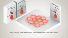
Graphene behaves as an electrical conductor due to the lack of a band gap , see the figure below for the energy of the electrons in graphene. However, an artificial band gap can be created in the graph by “cutting” a so-called gate with a maximum width of 10 nm into the layer .
Measurements have shown that a single layer of graphene attenuates the light by about πα ≈ 2.3% (with the fine structure constant α) over the entire visible spectrum .
Pseudo-relativistic behavior


The electrical properties of graphene can be easily described using a tight-binding model. In the context of this model, the energy of the electrons with wave number (see wave vector ) results to

- ,

with the nearest neighbor hopping energy and the lattice constant . The conduction and valence bands correspond to the plus and minus signs in the above dispersion relation . They touch each other in graphs at exactly six marked points, the so-called K-points, of which only two are independent of each other (the others are equivalent to these two due to the lattice symmetry). In their environment the energy depends like a relativistic particles linearly from (cf. photon. ). Since the base is diatomic, the wave function even has a formal spinor structure . This means that the electrons at low energies can be described by a relation that is equivalent to the Dirac equation , and that in addition in the so-called chiral limes , i.e. H. for vanishing mass , which results in some special features:


Here denotes the Fermi velocity in graphs, which takes the place of the speed of light; describes the Pauli matrices , the two-component wave function of electrons and their energy.


Unusual quantum Hall effect
Because of the peculiarities of the dispersion, the staircase structure of the integer quantum Hall plateaus , for all stages exactly "shifted by 1/2", the two-valley structure (formal "pseudospin") and the "real" Spin degeneracy together result in an additional factor 4. Remarkably, this can be observed - in contrast to the conventional quantum Hall effect - also at room temperature.


Stiffness and temperature dependence
Graphene is extremely stiff in the direction of the layers because the strength of the sp 2 bond between neighboring atoms is comparable to the sp 3 bond of diamond. Accordingly, one generally expects - and this corresponds to the experiment - that the properties of graphene that are interesting for the application do not only apply at absolute temperature zero, i.e. H. at −273.15 ° C, but remain valid at room temperature.
One such property is thermoelectricity : a temperature gradient in graphene levels causes an electric field strength due to a decoupling of the temperature of the electrons from that of the lattice. Electric tension in the illumination of graphene had been observed before, but photovoltaics was suspected to be the cause . The fact that the decoupling can still be observed at room temperature is due to the rigidity of the lattice: The elementary vibrational excitations of the lattice ( phonons ) are so high-energy that the electrons rarely generate such a phonon.
Elastic behavior and pseudo-magnetic field
In July 2010, a publication in the American scientific journal Science reported extremely strong pseudo magnetic fields . By elastic deformation, tiny triangular bubbles between 4 and 10 nanometers in size were created in graphene, in which the electrons moved as if they were being acted on by a magnetic field of around 300 Tesla . It turned out that the observed effect, in contrast to the effect of a real magnetic field, does not influence the actual spin of the electron , but that instead the just mentioned pseudo-spin is influenced, which is caused by the existence of two different equivalent base atoms in the honeycomb -Structure related. This pseudospin has a similar interaction with the pseudo-magnetic field as real spins with real magnetic fields, because these also generate "two-level systems". The experiments on the “pseudo-quantum Hall effect” generated in this way were based on theoretical predictions, which were thus confirmed.
Spin currents
In April 2011, A. Geim et al. Published an article in which they describe strong spin currents and current-induced magnetism near the Dirac point , i.e. H. near the meeting point of the conduction band and valence band. This opens up the prospect of applications in spintronics .
Chemical functionalization and major EU project
In 2013, the EU announced a new flagship project on graphenes, on which researchers in many Member States will collaborate, mainly physicists and chemists. You can z. B. Double bonds in graphene - every second bond is one - "break" and replace them with two single bonds to which various organic molecules are then attached: This allows the properties of the system to be specifically influenced.
Hydrodynamic behavior with unusual properties
In 2016, a so-called hydrodynamic (“liquid-like”) behavior of the electrons in the graph was found, but with extraordinary properties. B. The Wiedemann-Franz law , which is otherwise valid for metallic systems , that the ratio of thermal and electrical conductivity, divided by the Kelvin temperature T, is equal to a universal constant in metallic systems, is violated in graphs by approaching the Fermi energy to the point of intersection the thermal conductivity is much too large (the specific thermal resistance is much too small). In addition, one observes in this electronic fluid (technical term: Dirac fluid ) an unusual tendency towards the formation of vortex structures.
Generalizations
Generalizations are obvious. Some of the structures created by folding or rolling processes, including carbon nanotubes ( English carbon nanotubes ) and fullerenes , have already been mentioned. But it is more natural to first examine two-layer systems made of graphs. These have interesting additional properties: They show semiconducting behavior analogous to silicon , but with a band gap that can be systematically changed by electric fields.
Graphane
With the help of atomic hydrogen , which is generated by an electrical discharge in a hydrogen- argon mixture, graphene can be converted into graphane. In graphane, each carbon atom is assigned a hydrogen atom, and the bond structure is similar to that of chair-shaped cyclohexane . Above 450 ° C graphane breaks down into graphene and hydrogen. In contrast to graphene, graphane is an electrical insulator .
Double layer graph
Depending on the alignment of the two grids to one another, moiré patterns result with a correspondingly stronger coupling of the bands in both layers and new transport phenomena depending on the angle of rotation, which in 2011 led to the prediction of a new type of superconductivity by Allan H. MacDonald and Rafi Bistritzer at a certain angle of rotation led, experimentally confirmed by a team at the Massachusetts Institute of Technology under Pablo Jarillo-Herrero 2017. MacDonald, Bistritzer and Jarillo-Herrero received the Wolf Prize in Physics in 2020 .
Basic research and possible application
Because of the high electrical conductivity of graphene, research is currently being conducted into the question of whether graphene could replace silicon as a transistor material. The first successes such as the representation of a graphite microchip have already been achieved. With graph-based transistors, clock rates in the range of 500 to 1000 GHz should be possible. In early 2010, IBM succeeded in producing a 100 GHz graphene-based transistor for the first time. According to research by Yanqing Wu and co-workers from April 2011, carbon with a diamond structure appears to produce suitable substrates.
In basic research, graphene is used as a model substance for two-dimensional crystals: it is difficult to maintain the system in the form of individual layers ; It was not until 2004 that the first contactable “graphene flakes” could be obtained.
- Possible use in supercapacitors and batteries
- As graphene oxide, it is gas-tight and at the same time permeable to H 2 O molecules. This makes it suitable for use as a water filter, distillator and sealant, especially as a hermetic seal (even tight for helium).
- Possible use in photovoltaics as a third generation solar cell with an efficiency of up to 60%. However, according to recent research, this approach does not appear to be possible.
- Realization of a stable and durable memory cell for artificial neural networks with intermediate states instead of binary values
In 2013, as part of the European Flagship Initiative , the European Commission decided to fund research into graphene with 1 billion euros.
In November 2016 a new possibility was reported to use graphene as a kind of mechanical pixel for the development of new energy efficient color displays. A graphene membrane over an air chamber arches when there are pressure differences and incident light is reflected in different colors. The researchers believe that this can be used to develop a reflective display technology based on interferometric modulation .
The Fraunhofer Institute for Organic Electronics, Electron Beam and Plasma Technology (FEP) succeeded for the first time in 2016/17 in producing OLED electrodes from graphene. The process was developed and optimized in the EU-funded project "Gladiator" (Graphene Layers: Production, Characterization and Integration) together with partners from industry and research.
The Australian company Talga is developing a new type of concrete that will, among other things, promote electric mobility. The concrete is mixed with graphene. This should enable inductive charging of electric cars or the heating of the street.
Effects on humans and the environment
As of 2014, only very small amounts of graphene have been produced - mostly in very small amounts for purely scientific purposes. The toxicity of graphene has not yet been investigated in depth, nor has its possible impact on the environment. Scientists at the University of California, Riverside believe that research into the dangers of graphene is equivalent to that of pharmaceutical and chemical science 30 years ago. First publications on this topic suggest, among other things, that graphene has a high mobility in groundwater and could therefore spread quickly.
See also
literature
- Björn wedding slip: From graphite to graphene . In: Physics Journal . tape 6 , no. 7 , 2007, p. 39–44 ( pro-physik.de ).
- Mikhail Katsnelson : Graphene: carbon in two dimensions . In: Materials Today . tape 10 , no. 1–2 , 2007, pp. 20-27 , doi : 10.1016 / S1369-7021 (06) 71788-6 .
- Mikhail I. Katsnelson: Graphene. Carbon in two dimensions. Cambridge University Press, Cambridge u. a. 2012, ISBN 978-0-521-19540-9 .
- Phaedon Avouris, Zhihong Chen, Vasili Perebeinos: Carbon-based electronics . In: Nat Nano . tape 2 , no. 10 , 2007, p. 605-615 , doi : 10.1038 / nnano.2007.300 .
- Andre K. Geim , Philip Kim: Wonder material from the pencil . In: Spectrum of Science . No. 8 , 2008, p. 86-93 .
- AH Castro Neto, F. Guinea, NMR Peres, KS Novoselov , AK Geim: The electronic properties of graphene . In: Reviews of Modern Physics . tape 81 , no. 1 , 2009, p. 109–154 , doi : 10.1103 / RevModPhys.81.109 , arxiv : 0709.1163v2 (review article).
- AC Ferrari et al .: Science and technology roadmap for graphene, related two-dimensional crystals, and hybrid systems . In: Nanoscale . tape 7 , no. 11 , 2015, p. 4598–4810 , doi : 10.1039 / C4NR01600A (review article of the EU flagship initiative on the technical status, English, open access).
Web links
- Jan Oliver Löfken: Graphs: Perhaps the most stable paper in the world. In: pro-physik.de. July 26, 2007, accessed March 28, 2008 .
- Thomas Pichler: Smallest transistor in the world, only one atom thick. In: Press text Switzerland (pte). April 18, 2008, accessed March 28, 2008 .
- All publications of A. Geim's group on graphs can be downloaded here individually (in English). (No longer available online.) In: The University of Manchester. 2007, archived from the original on April 30, 2008 ; accessed on November 28, 2016 .
- Information on graphs and in-depth discussion on the discovery question (in English). (No longer available online.) In: Graphene Times. Archived from the original on April 20, 2010 ; accessed on November 28, 2016 .
- Made in IBM Labs: IBM Scientists Demonstrate World's Fastest Graphene Transistor . February 5, 2010 (English; IBM develops a 100 GHz transistor based on graphs)
- Is graphene a miracle material? ("Many believe it could spell the end for silicon and change the future of computers and other devices forever"), Alex Hudson, BBC News, May 21, 2011.
- Ansgar Kretschmer: Wonder material in two dimensions . May 15, 2014 (Scinexx dossier).
References and footnotes
- ↑ LD Landau : On the theory of phase transitions II . In: Phys. Z. Soviet Union . tape 11 , 1937, pp. 11 .
- ^ RE Peierls : Quelques propriétés typiques des corpses solides . In: Ann. IH Poincaré . tape 5 , 1935, pp. 177-222 .
- ↑ a b K. S. Novoselov, AK Geim, SV Morozov, D. Jiang, Y. Zhang, SV Dubonos, IV Grigorieva, AA Firsov: Electric Field Effect in atomically thin carbon film . In: Science . tape 306 , no. 5696 , 2004, pp. 666-669 , doi : 10.1126 / science.1102896 .
- ^ ND Mermin: Crystalline Order in Two Dimensions . In: Physical Review . tape 176 , no. 1 , 1968, p. 250 ff ., doi : 10.1103 / PhysRev.176.250 .
- ↑ JC Meyer, AK Geim, MI Katsnelson, KS Novoselov, TJ Booth, S. Roth: The structure of suspended graphene sheets . In: Nature . tape 446 , 2007, pp. 60–63 , doi : 10.1038 / nature05545 .
- ↑ a b See e.g. B. Cover picture and p. 22 of the “Physik Journal” 12 / Dec. 2010, online .
- ^ Manfred Lindinger: Nobel Prize for Physics 2010. The skid marks of the pencil . FAZ.net, October 5, 2010, accessed on October 5, 2010. (Unfortunately the newspaper switched the photos: the man in the black sweater is K. Novoselov and not A. Geim)
- ^ A b P. R. Wallace: The Band Theory of Graphite . In: Physical Review . tape 71 , no. 9 , 1947, pp. 622-634 , doi : 10.1103 / PhysRev.71.622 .
- ^ Sumio Iijima : Helical microtubules of graphitic carbon . In: Nature . tape 354 , 1991, pp. 56-58 , doi : 10.1038 / 354056a0 .
- ↑ Mitsutaka Fujita, Riichiro Saito, G. Dresselhaus, MS Dresselhaus : Formation of general fullerenes by their projection on a honeycomb lattice . In: Physical Review B . tape 45 , no. 23 , 1992, pp. 13834-13836 , doi : 10.1103 / PhysRevB.45.13834 .
- ↑ Patrick Vogt u. a .: Silicene: Compelling Experimental Evidence for Graphenelike Two-Dimensional Silicon . In: Physical Review Letters . tape 108 , no. 15 , April 12, 2012, p. 155501 , doi : 10.1103 / PhysRevLett.108.155501 .
- ^ Benjamin C. Brodie: On the Atomic Weight of Graphite . In: Proceedings of the Royal Society of London . tape 10 , 1859, p. 249 , JSTOR : 108699 .
- ^ V. Kohlschütter, P. Haenni: On the knowledge of graphitic carbon and graphitic acid . In: Journal of Inorganic and General Chemistry . tape 105 , no. 1 , 1918, p. 121-144 , doi : 10.1002 / zaac.19191050109 .
- ↑ G. Ruess and F. Vogt: Highest lamellar carbon from graphite oxyhydroxide. In: Monthly magazine for chemistry . tape 78 , no. 3–4 , 1947, pp. 222-242 .
- ↑ HP Boehm, A. Clauss, GO Fischer, U. Hofmann: The adsorption behavior of very thin carbon foils . In: Journal of Inorganic and General Chemistry . tape 316 , no. 3-4 , 1962, pp. 119-127 , doi : 10.1002 / zaac.19623160303 .
- ↑ HP Boehm, R. Setton, E. Stumpp: Nomenclature and terminology of graphite intercalation compounds . In: Pure and Applied Chemistry . tape 66 , no. 9 , 1994, pp. 1893-1901 .
- ↑ Savage: Super Carbon, 2012, p. 30.
- ^ WA Harrison: Electronic structure and the properties of solids: the physics of the chemical bond . WH Freeman and Company, San Francisco 1980.
- ↑ For the π-states see z. BCE Mortimer: Chemistry . 9th edition. Georg Thieme Verlag , Stuttgart 2007, ISBN 978-3-13-484309-5 .
- ↑ Andreas Wilkens: Graphs: The miracle material now also from the kitchen mixer . heise online, accessed on April 23, 2014.
- ↑ J. Wu, W. Pisula, K. Mullen: graphenes as potential material for electronics . In: Chemical Reviews . tape 107 , no. 3 , 2007, p. 718-747 , doi : 10.1021 / cr068010r .
- ↑ L. Zhi, K. Müllen: A bottom-up approach from molecular nanographenes to unconventional carbon materials . In: J. Mater. Chem. Band 18 , no. 18 , 2008, p. 1472-1484 , doi : 10.1039 / b717585j .
- ↑ Y. Hernandez, V. Nicolosi, M. Lotya, F. Blighe, Z. Sun, S. De, IT McGovern, B. Holland, M. Byrne, Y. Gunko, J. Boland, P. Niraj, G. Duesberg, S. Krishnamurti, R. Goodhue, J. Hutchison, V. Scardaci, AC Ferrari, JN Coleman: High yield production of graphene by liquid phase exfoliation of graphite . In: arXiv . 2008, arxiv : 0805.2850 .
- ↑ Mohammad Choucair, Pall Thordarson, John A. Stride: Gram-scale production of graphene based on solvothermal synthesis and sonication . In: Nature Nanotechnology . tape 04 , 2009, p. 30-33 , doi : 10.1038 / NNANO.2008.365 .
- ↑ P. Steurer, R. Wissert, R. Thomann, R. Mülhaupt: Functionalized Graphenes and Thermoplastic Nanocomposites Based upon Expanded Graphite Oxide. In: Macromolecular Rapid Communications. Volume 30. WILEY-VCH Verlag, 2009, pp. 316–327.
- ↑ AT N'Diaye, S. lead Kamp, PJ Feibelman, T. Michely: Two-Dimensional Ir cluster lattice on a Moiré Graphene on Ir (111) . In: Physical Review Letters . tape 97 , no. 21 , 2006, p. 718-747 , doi : 10.1103 / PhysRevLett.97.215501 .
- ↑ PW Sutter, J.-I. Flege, EA Sutter: Epitaxial graphene on ruthenium . In: Nature Materials . tape 97 , no. 5 , 2008, p. 406-411 , doi : 10.1038 / nmat2166 .
- ↑ I. Forbeaux, J.-M. Themlin, J.-M. Debever: Heteroepitaxial graphite on 6H-SiC (0001): Interface formation through conduction-band electronic structure, overview surface reconstructions LEED, KRIPES, dispersion relation, XPS, UPS, SXPS . In: Physical Review B . No. 24 , 1998, pp. 16396-16406 , doi : 10.1103 / PhysRevB.58.16396 .
- ↑ A. Charrier, A. Coati, T. Argunova, F. Thibaudau, Y. Garreau, R. Pinchaux, I. Forbeaux, J.-M. Debever, M. Sauvage-Simkin, J.-M. Themlin: Solid-state decomposition of silicon carbide for growing ultra-thin heteroepitaxial graphite films . In: Journal of Applied Physics . tape 92 , no. 5 , 2002, p. 2479-2480 , doi : 10.1063 / 1.1498962 .
- ↑ KV Emtsev, A. Bostwick, K. Horn, J. Jobst, GL Kellogg, L. Ley, JL McChesney, T. Ohta, SA Reshanov, E. Rotenberg, AK Schmid, D. Waldmann, HB Weber, Th. Seyller : Atmospheric pressure graphitization of SiC (0001) - A route towards wafer-size graphene layers . In: arXiv - Condensed Matter, Materials Science . 2008, arxiv : 0808.1222 .
- ↑ Sukang Bae, Hyeongkeun Kim, Youngbin Lee, Xiangfan Xu, Jae-Sung Park, Yi Zheng, Jayakumar Balakrishnan, Tian Lei, Hye Ri Kim, Young Il Song, Young-Jin Kim, Kwang S. Kim, Barbaros Ozyilmaz, Jong- Hyun Ahn, Byung Hee Hong, Sumio Iijima: Roll-to-roll production of 30-inch graphene films for transparent electrodes . In: Nat Nano . tape 5 , no. 8 , 2010, p. 574-578 , doi : 10.1038 / nnano.2010.132 ( PDF [accessed October 5, 2010]). PDF ( Memento of the original from July 10, 2012 in the Internet Archive ) Info: The archive link was inserted automatically and has not yet been checked. Please check the original and archive link according to the instructions and then remove this notice.
- ↑ Luca Banszerus, Michael Schmitz, Stephan Engels, Jan Dauber, Martin Oellers, Federica Haupt, Kenji Watanabe, Takashi Taniguchi, Bernd Beschoten and Christoph Stampfer: Ultrahigh-mobility graphene devices from chemical vapor deposition on reusable copper . In: Sci Adv . tape 1 , no. 6 , 2015, p. e1500222 , doi : 10.1126 / sciadv.1500222 ( PDF [accessed on August 8, 2015]).
- ↑ Wang, Yu et al .: Electrochemical Delamination of CVD-Grown Graphene Film. Toward the Recyclable Use of Copper Catalyst, in: ACS Nano Vol. 5, No. 12, No. 2011. pp. 9927-9933.
- ^ JO Löfken: Ultrafast graph growth. Retrieved October 25, 2016.
- ^ A b c Harry Marsh, Francisco Rodríguez-Reinoso: Science of Carbon Materials . 2000. Quoted in: Christian Anton Rottmair: Influence of thermal process control on the properties of graphite molded parts , produced by powder injection molding of mesophase carbon . 2007, p. 10–11 ( PDF - dissertation, University of Erlangen-Nuremberg, 2007).
- ↑ a b c d Changgu Lee, Xiaoding Wei, Jeffrey W. Kysar, James Hone: Measurement of the Elastic Properties and Intrinsic Strength of Monolayer Graphene . In: Science . tape 321 , no. 5887 , 2008, p. 385-388 , doi : 10.1126 / science.1157996 .
- ↑ a b Rainer Scharf: Visible fine structure constant. (No longer available online.) In: Pro Physik. April 4, 2008, archived from the original on December 18, 2010 ; Retrieved February 24, 2011 . Info: The archive link was inserted automatically and has not yet been checked. Please check the original and archive link according to the instructions and then remove this notice.
- ^ Class for Physics of the Royal Swedish Academy of Sciences: Scientific Background on the Nobel Prize in Physics 2010 - Graphene . 2010, p. 8 ( PDF ).
- ↑ Ansgar Kretschmer: Never again cracks in the smartphone display. In: Graphs. Wonder material in two dimensions. May 15, 2014, p. 5 , accessed on January 12, 2011 (Scinexx dossier).
- ↑ Nico Ernst: British develop one-electron transistor from graphene: two-dimensional carbon as a new semiconductor. In: www.golem.de. Golem.de, March 6, 2007, accessed on November 28, 2016 .
- ↑ Kevin Bullis, Wolfgang Stieler: Magical semiconductor material . In: Technology Review . tape 4 , 2008 ( online [accessed March 28, 2008]).
- ↑ Zhihong Chen, Yu-Ming Lin, Michael J. Rooks, Phaedon Avouris: Graphene nano-ribbon electronics . In: Physica E: Low-dimensional Systems and Nanostructures . tape 40 , no. 2 , 2007, p. 228-232 , doi : 10.1016 / j.physe.2007.06.020 .
- ↑ Mike Rodewalt: Researchers discover method for mass production of nanomaterial graphene. In: UCLA Newsroom. November 10, 2008, accessed November 16, 2008 .
- ^ AB Kuzmenko, E. van Heumen, F. Carbone, D. van der Marel: Universal infrared conductance of graphite . In: Phys Rev Lett . Vol. 100, No. 11 , 2008, p. 117401 , doi : 10.1103 / PhysRevLett.100.117401 , PMID 18517825 , bibcode : 2008PhRvL.100k7401K .
- ↑ RR Nair et al. a .: Fine Structure Constant Defines Visual Transparency of Graphene . In: Science . tape 320 , no. 5881 , June 6, 2008, p. 1308–1308 , doi : 10.1126 / science.1156965 ( PDF ).
- ↑ B. Wedding note: From graphite to graphene . In: Physics Journal . 2007.
- ↑ a b A. H. Castro Neto, F. Guinea, NM R Peres, KS Novoselov , AK Geim : The electronic properties of graphene . In: Arxiv preprint . 2007, arxiv : 0709.1163v2 .
- ↑ a b A. K. Geim, K. S. Novoselov: The rise of graphene . In: Nature Materials . No. 6 , 2007, p. 183-191 , doi : 10.1038 / nmat1849 .
- ^ KS Novoselov, AK Geim, SV Morozov, D. Jiang, MI Katsnelson, IV Grigorieva, SV Dubonos, AA Firsov: Two-dimensional gas of massless Dirac fermions in graphene . In: Nature . tape 438 , no. 7065 , 2005, pp. 197-200 , doi : 10.1038 / nature04233 , arxiv : cond-mat / 0509330v1 .
- ↑ Nathaniel M. Gabor, Justin CW Song, Qiong Ma, Nityan L. Nair, Thiti Taychatanapat, Kenji Watanabe, Takashi Taniguchi, Leonid S. Levitov, Pablo Jarillo-Herrero: Hot Carrier – Assisted Intrinsic Photoresponse in Graphene . In: Science . No. 6056 , 2011, pp. 648-652 , doi : 10.1126 / science.1211384 .
- ^ N. Levy, SA Burke, KL Meaker, M. Panlasigui, A. Zettl, F. Guinea, AH Castro Neto, MF Crommie: Strain-Induced Pseudo-Magnetic Fields Greater Than 300 Tesla in Graphene Nanobubbles . In: Science . tape 329 , no. 5991 , June 30, 2010, p. 544-547 , doi : 10.1126 / science.1191700 .
- ↑ In the language of chemistry: There are two equivalent possibilities to alternately introduce single and double bonds in a six-membered ring ("benzene ring").
- ↑ DA Abanin, SV Morozov, LK Ponomarenko, RV Gorbachev, AS Mayorov, MI Katsnelson, K. Watanabe, T. Taniguchi, KS Novoselov, LS Levitov, AK Geim: Giant Nonlocality Near the Dirac Point in Graphene . In: Science . tape 332 , no. 6027 , April 15, 2011, p. 328-330 , doi : 10.1126 / science.1199595 .
- ↑ See e.g. For example, the following article in the May 2011 edition of the Physik-Journal: Online ( Memento of the original from May 22, 2011 in the Internet Archive ) Info: The archive link was inserted automatically and has not yet been checked. Please check the original and archive link according to the instructions and then remove this notice. .
- ↑ See, for example, the article by Louisa Knobloch, researchers rely on “Wundermaterial” , Mittelbayerische Zeitung, Feb. 11, 2013, page 21, or the following Internet article from the University of Erlangen, EU starts new major project in the field of graphs , (accessed on 11 February 2013)
- ↑ Alexander D. Mirlin and Jörg Schmalian: Electrons in the Flow , Physik Journal 15 (5), 18-19 (2016)
- ↑ Yuanbo Zhang, Tsung-Ta Tang, Caglar Girit, Zhao Hao, Michael C. Martin, Alex Zettl, Michael F. Crommie, Y. Ron Shen, Feng Wang: Direct observation of a widely tunable bandgap in bilayer graphene . In: Nature . tape 459 , no. 7248 , 2009, p. 820–823 , doi : 10.1038 / nature08105 .
- ↑ DC Elias, RR Nair, TMG Mohiuddin, SV Morozov, P. Blake, MP Halsall, AC Ferrari, DW Boukhvalov, MI Katsnelson, AK Geim, KS Novoselov: Control of Graphene's Properties by Reversible Hydrogenation: Evidence for Graphane . In: Science . tape 323 , no. 5914 , September 30, 2009, p. 610-613 , doi : 10.1126 / science.1167130 .
- ^ David Chandler: New material could lead to faster chips. In: MIT News . March 19, 2009. Retrieved March 28, 2009 .
- ↑ Made in IBM Labs: IBM Scientists Demonstrate World's Fastest Graphene Transistor. IBM press release dated February 5, 2010
- ↑ Yanqing Wu, Yu-ming Lin, Ageeth A. Bol, Keith A. Jenkins, Fengnian Xia, Damon B. Farmer, Yu Zhu, Phaedon Avouris: High-frequency, scaled graphene transistors on diamond-like carbon . In: Nature . tape 472 , no. 7341 , March 7, 2011, p. 74-78 , doi : 10.1038 / nature09979 .
- ↑ Researchers develop graphene supercapacitor holding promise for portable electronics
- ↑ The University of Manchester "Supermaterial goes superpermeable"
- ↑ The new coal power
- ↑ Research, Updates, 2013, Graphene is suitable as an active material for a terahertz laser
- ↑ With graphs for the optimized memory cell
- ↑ European Flagship Initiative (tabular overview of the European Commission)
- ↑ Angela Meyer: Researchers develop new types of mechanical pixels. In: heise.de. Heise Online, November 27, 2016, accessed November 28, 2016 .
- ↑ New high-tech material: Milestone in graphene production - press release from FEP. fep.fraunhofer.de, January 3, 2017, accessed on January 8, 2017 .
- ↑ Conductive concrete enables electric vehicles to be charged. June 27, 2018, accessed July 1, 2018 .
- ↑ Jacob D. Lanphere, Brandon Rogers, Corey Luth, Carl H. Bolster, Sharon L. Walker: Stability and Transport of Graphene Oxide Nanoparticles in Groundwater and Surface Water . In: Environmental Engineering Science . March 17, 2014, doi : 10.1089 / ees.2013.0392 .