Circuit board
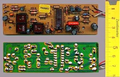
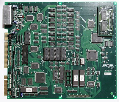
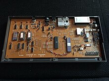
A printed circuit board ( PCB , board or printed circuit ; English printed circuit board , PCB ) is a carrier for electronic components . It is used for mechanical fastening and electrical connection. Almost every electronic device contains one or more printed circuit boards.
Circuit boards consist of electrically insulating material with conductive connections (conductor tracks) adhering to them. Fiber-reinforced plastic , or hard paper for cheaper devices , is the usual insulating material . The conductors are usually made of a thin layer of copper , usually 35 microns, etched . The components are soldered on soldering surfaces (pads) or in soldering eyes . In this way, they are held mechanically and electrically connected to these footprints at the same time. Larger components can also be attached to the circuit board with cable ties , glue or screw connections .
PCB types
The types of circuit boards range from single-sided circuit boards to multilayers and special technologies.
- Standard PCBs
- Single sided and double sided PCBs
- Multilayer with several layers (different, depending on the manufacturer)
- Special techniques (special techniques are used in all branches of industry and have special properties and requirements)
- Flexlam
- High current: To implement the transport of high currents and signal electronics via a printed circuit board.
- Thick copper
- Thin circuit boards
- Slip ring: A slip ring is used for the transmission and tapping of energy, signals and data in rotating systems. Areas of application are, for example, in industrial robots and wind turbines. Correct application of the precious metal coating is a prerequisite for the reliability and service life of a slip ring surface.
- HDI circuit board
- IMS circuit board
- Circuit boards on glass
Manufacturing
draft
The circuit board design (layout) is now mostly done with software that contains not only the circuit data but also the circuit diagram and often parts lists as well as data such as solder paste samples or assembly printing . The circuit board design can be output from the circuit board layout programs in a standard format. Most circuit board manufacturers process the Gerber RS-274X , Excellon or Sieb & Meyer formats . The project data of the circuit board are split up. The first part consists of Gerber data for the topography of the circuit boards. This z. B. the conductor path and the localization of PADs etc. are documented. The second part consists of the drilling data in the format of Excellon or Sieb & Meyer data.
The PCB layout (manually or with an autorouter ) is the main content of the design. There is also technological information such as copper thickness, circuit board manufacturing technology and surface type. The data is now transferred to the circuit board manufacturer.
- CAM
The circuit board manufacturer will first read the data into a CAM station. In the CAM station, a layer structure is first created from the data so that the function of the data is known to the system. Design rule checks are then used to check whether the data supplied can actually be produced. Once this step has been overcome, a production panel can be created. From here it is then possible to generate programs required for production. This includes outputs for film plotters / imagers, drilling, milling and scribing data, AOI (Automatic Optical Inspection) outputs, electrical test programs, and much more.
The production data is structured in levels separated by function:
- Sample of one or more copper layers (conductors and surfaces)
- Drill holes (position, depth and diameter)
- Outline and breakthroughs
- Assembly plan above and below
- Solder mask on top and bottom
- Placement print on top and bottom
- Adhesive dots and solder paste patterns for SMD components above and below
- Partial metallization (e.g. gold plating for contact surfaces)
Series production
- Photochemical process
The majority of single-sided and double-sided plated-through circuit boards are produced photochemically.
The current order of the manufacturing steps is:
- Drill
- Through-hole plating (for double-sided circuit boards)
- Laminate photoresist
- Expose
- Develop
- etching
- do the washing up
- dry
This is followed by post-processing steps as required.
Originally, the drilling and through-hole plating was only after the etching made the PCB. But since the photoresist was replaced by so-called dry resist, a photosensitive film, the order of the production steps has changed. The advantage is that a mask no longer has to be applied to the circuit board before the through-hole plating, which prevents the copper from growing in undesired places. Since the entire printed circuit board is still covered by copper at this point, only the layer thickness of the copper foil increases. The metallized holes are closed on both sides by the photoresist film during the etching process.
The conductor tracks are usually produced photolithographically by applying a thin layer of light-sensitive photoresist to the surface of the plate, which is still completely metallized. After the photoresist has been exposed through a mask with the desired circuit board layout, depending on the photoresist used, either the exposed or the unexposed portions of the lacquer are soluble in a suitable developer solution and are removed. If the printed circuit board treated in this way is placed in a suitable etching solution (e.g. iron (III) chloride or sodium persulfate dissolved in water or with hydrochloric acid + hydrogen peroxide ) only the exposed part of the metallized surface is attacked; the parts covered by the photoresist are retained because the lacquer is resistant to the etching solution.
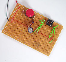
Prototypes can also be structured by milling the copper layers ("isolation milling ", see picture below for soldering grid boards). Such circuit boards do not consist of conductor tracks, but of surfaces that are separated from one another by milling tracks.
The copper layers can be galvanically reinforced after the etching .
The production of the bores for receiving wired components as well as for vias requires hard metal tools due to the glass fiber content of the carrier material. When holes are metallized on the inner walls, vias are created. The metallization of the bores (insulating surfaces) requires germination, subsequent electroless deposition of a thin copper layer and finally its electrolytic reinforcement.
In addition, metallic protective and contact layers made of tin , nickel or gold can be applied galvanically on partial areas or the entire copper area. Thin gold plating requires a diffusion barrier layer (nickel barrier layer) towards the copper.
Then a solder mask (green lacquer layer on the circuit board in the photo) is applied, which covers the conductor tracks and only leaves the solder points free. This avoids soldering errors, wave soldering saves tin and the conductor tracks are protected from corrosion. The remaining free soldering points (pads and soldering eyes) can be coated with a layer of tin using a physical process ( hot air leveling ) and additionally with a flux , which enables better soldering.
Solder paste islands for soldering SMD components are applied using a solder paste mask. It is made of sheet metal and has holes where solder paste is to be applied. The masks are made by fine laser cutting . Another possible process step in SMD assembly is the application of adhesive dots, which ensure the fixation of the components during assembly (pick and place) through to soldering.
Circuit boards often have an assembly print produced by screen printing, which, in conjunction with a circuit diagram, facilitates assembly and service.
- Stamping technology and wire-laying technology
- Two other important manufacturing processes for printed circuit boards are stamping technology and wire laying technology.
Printed circuit boards are manufactured for very large quantities using stamping technology. The technology is only suitable for single-sided printed circuit boards made of Pertinax or unreinforced plastics. Base material without a copper layer is used, a copper foil with an adhesive layer is placed on the base material and then the conductor tracks are punched out with an embossing die and simultaneously pressed onto the base material. The contour of the circuit board and the holes are punched, and the conductor pattern is punched out and glued to the base material in one operation.
The wire-laying technique is used for small series and for special applications that require the circuit board to withstand high currents. A machine lays insulated wires on the base material, which are connected to the soldering points using ultrasonic welding and attached to the surface of the base material.
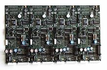
In the production of printed circuit boards, the term “benefit” refers to the combination of several smaller layouts on one large circuit board. The term comes from printing technology . The entire processing chain is carried out with this benefit as far as possible. By cleverly arranging different designs, the usually rectangular formats of the base material can also be used effectively with different, for example L-shaped, geometries. The term panel separation is used for the subsequent necessary division of the board .
- screen printing
- Instead of the photochemical process, the screen printing technique can also be used to cover the conductor tracks before etching . This is particularly suitable for material coated on one side and for circuit boards with a low level of difficulty.
Prototypes
Before mass production, it is often advisable to test a circuit without risking the high cost of creating the photomasks.
There are the following options:
- Experiment boards
Hole grid boards have holes or soldering eyes (one-sided or plated through) in a grid that is common for electronic components, i.e. 2.54 mm, which corresponds to 0.1 inches (for the rarer metric components 2.5 mm) or half of it. Connections can be made by soldering with jumper wire , using threading technology , using winding technology or simply by plugging in. Often several eyes are already connected by conductor tracks (e.g. for operating voltages) or longer and shorter conductor tracks are provided in order to come closer to practical requirements. Experimental boards (solder strip boards) completely provided with parallel conductor tracks are also common. If required, these can be separated with a tool by scratching the conductor path. There are also small experimental boards suitable for common SMD housing shapes in order to adapt their connections to the grid.
- Manufacturing in the pool
Manufacturers offer the production of individual items and small series in the "pool", i. H. several individual pieces as use (see above) are drilled, plated through, exposed, etched and then milled out on a large plate.
- Milling technology
With the milling technique, dividing lines are created between the conductor surfaces with a pin milling cutter. All copper remains in place (island process). The wet chemical and photolithographic steps are omitted. CNC programs can be generated with special CAD software so that even prototypes can be produced quickly.
- Toner transfer method
The layout is printed mirror-inverted with a laser printer on suitable paper or a specially made heat-resistant film (catalog pages or similar) and then "ironed" onto the circuit board with an iron or laminator. The toner as in the case fixing unit of the printer slightly liquid and combines with the copper of the board. The paper is then removed again with water - the toner remains on the copper. This is followed by the etching process, whereby the areas covered by the toner remain. The toner can then be removed with thinner. With this process, tolerances can occur due to paper transport in the printer and due to stretching and shrinking of the paper due to heating.
- Felt-tip pens
The conductor tracks and soldering eyes can also be transferred directly to the base material with a waterproof felt pen (so-called permanent marker). The paint protects the covered surfaces during the etching process. After the etching, the color is then removed with alcohol or acetone .
If this process is applied analogously to a plastic film, the resulting mask can also be used for the photo-positive process and in this way enables mass production.
- Rub-on symbols
Some manufacturers sell rub-in symbols that represent soldering eyes, conductor track parts or electrical symbols. These are - similar to decals - placed on the circuit board and rubbed. The applied symbols then protect the copper underneath them during the etching process. This method is also used in combination with a felt-tip pen (e.g. soldering eyes with rub-in symbols, conductor tracks with a felt-tip pen). After etching, the symbols are removed by acetone or by scraping. Soldering varnish , which is often applied to improve the flow properties of the solder, also removes the symbols.
This method can also be applied to a film for the photo positive method for mass production.
- Oil method
The oil method is particularly popular with hobbyists for the quick implementation of designs with minimal effort. The layout is printed out on normal paper with the highest level of darkness and then soaked in oil, making the paper largely transparent. The actual exposure can be carried out with any UV light source (sun, solarium, ...).
history

Before the introduction of printed circuit boards, electronic circuits were freely wired, possibly with the additional use of soldering strips . Mechanical support points were components such as potentiometers , variable capacitors , switches with their soldering lugs and the sockets of electron tubes . Depending on the manufacturer, efforts were made to arrange the components at right angles or to always choose the direct, inclined connection. Since the components such as capacitors or resistors were also very large and long at the time, they were able to bridge distances of a few centimeters.
Devices of this type could only be manufactured by hand and with knowledge of the wiring plan.
PCB forerunners from the 1920s onwards were punched conductor tracks that were riveted onto hard paper. Components (resistors, capacitors) were carried between sheet metal springs without a soldered connection. Paul Eisler , a Viennese electronics engineer, patented the principle of the printed circuit board in 1943, but for a long time it had a rather insignificant shadowy existence alongside the regular manual wiring. It was only with the increasing miniaturization of electronics that the importance of this technology increased.
In the early days around 1940, circuits were also produced by screen printing conductive silver lacquer on the base plate. On the other hand, conductive paths and resistors that are printed and burned into ceramic substrates are referred to as thick-film technology .
manufacturing engineering
The use of printed circuit boards began in the early 1950s through the Ruwel-Werke founded by Fritz Stahl in Geldern on the Lower Rhine .
In the case of printed circuits, the connection wires of the components are inserted from above through drill holes through the circuit board ( Through Hole Technology , THT ) - a technology that is still widespread today. On the underside (solder, conductor or L-side) are the copper conductor tracks to which they are soldered. This allows a simplified and automatable production, at the same time the error rate in the production decreases, since wiring errors are excluded for the circuit on the circuit board.
More complex single-layer circuit boards require additional connections that cannot be made in the layout. These are made by solder bridges using angled wires or zero ohm resistors. The latter can be better used in pick and place machines . Alternatively, copper tracks are used for these connections on both sides of the circuit board (double-layer circuit board, DL). Connections between the upper (component or B-side) and the lower side were created by soldering pressed-in pins or rivets.
It was not until the 1960s that these connections ( plated-through holes , DK, English vias ) were produced chemically through the circuit board by metallizing the hole walls of the bores.
For cost reasons, single-layer printed circuit boards are still produced today if the circuit allows it. Compared to a double-sided, plated-through circuit board, the costs for a single-sided circuit board of the same size are 25–50%.
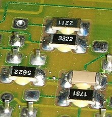
A significant part of the printed circuit boards manufactured worldwide is still assembled by hand today, although assembly machines have been around since the mid-1970s. However, modern printed circuit boards with a high packing density and surface-mountable components ( SMD ) can only be partially assembled by hand. So-called "pick & place" machines handle the sometimes less than 1 mm² components. After the reflow soldering of the SMD on both sides, the THT components are increasingly being assembled by hand and then selectively soldered. With the exception of QFN , BGA and very small 0201 milli-inch components, almost all SMD components can be soldered by hand without any problems. Soldering by hand is problematic when it comes to power components (regardless of the design) with a large pad on the underside for heat dissipation. These power components as well as QFN and BGA components can possibly still be soldered by hand, for example with a heat gun . However, the component or components in the vicinity can be damaged if it is heated for too long.
layout
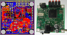
In the 1960s, the layout (conductor track structure) was drawn on a scale of 2: 1 with ink or using adhesive technology with layout symbols and adhesive rolls (Brady) on grid foils. Later NC programs were created at programming workstations to control a light drawing device, which produced the film required for photolithography. Then computers were used to generate the drawings of the various copper and pressure layers as well as the NC control program for producing the holes.
Current layout programs for the so-called Electronic Design Automation (EDA) enable the generation of a connection plan and the corresponding representation ("rat's nest") from a circuit diagram and contain extensive component libraries in which the housing geometries, technical data and the position for each component and size of the soldering pads ( English footprint , for "footprint") are included. The footprint denotes the dimensions of the soldering eyes in Through Hole Technology (THT) or the dimensions of the soldering pads in Surface Mounted Devices (SMD) for a specific component on the circuit board.
The automatic circuit board unbundling based on a given circuit diagram and specification of design rules (placement of components ( autoplacement ) and unbundling ( autorouting ) of electrical connections) is standard for simple circuit boards today. This process reaches its limits with complex printed circuit boards that require a lot of experience in unbundling (e.g. with cell phones). Even an increase in the computer processing power does not bring any improvement, since entering the complex design specifications sometimes takes more time than manual unbundling.
The current carrying capacity ( current density ) of conductor tracks is an important design aspect. It can be significantly higher than that of solid wires, as the substrate cools through heat conduction. Layout software can take the current carrying capacity into account.
Other aspects are:
- At high frequencies and pulse steepnesses, the wave impedance of the conductor tracks is important (see strip line ).
- In the case of digital circuits with a high clock frequency, care must be taken that interconnects (bus) that belong together are of the same length so that the signals arrive at the end of the interconnects at the same time.
- With analog signals (especially audio applications with a high dynamic range), ground loops (also known as ground loops, hum loops) must be avoided.
- With high electrical voltages, certain minimum distances (aura) must be observed between the conductor tracks for safety reasons. Thus, in optocouplers , the signals separated circuits galvanically isolated link, which in accordance with regulations tracking resistance increased by the pins of the DIP package are spread or the circuit board is durchgefräßt under the component.
EMC-compliant layout
The capacitive and inductive coupling of the conductor tracks, their sensitivity to external electromagnetic fields and the radiation characteristics (interference emission) are described under the collective term electromagnetic compatibility (EMC). Modern software can now to some extent also take EMC aspects into account within the board.
An EMC-compliant circuit board layout becomes necessary with stricter regulations on interference radiation. The shortest possible conductor tracks, which cannot function as an antenna, as well as the possible parallel return of the currents of high-frequency and power-intensive signals or their operating voltage apply. Main boards like the K7S5A from 2001, which was produced sparingly with only four layers, as well as the Gigatron TTL learning computer, which was experimentally constructed as a 2 and 4 layer, show an interesting EMC behavior, in that one layer each is available as a circuit board-wide mass and operating voltage. These layers act with one another and with the signal lines running above and below it as a permanent low-pass filter , which leads to an offset-like lowering of the background noise caused by the circuit. Electrically tight housings have similar effects for the frequency . In the case of switched-mode power supplies , the transmitted impulse must be sufficiently filtered and buffered. Longer signal lines can only be filtered to prevent coupling to other lines if possible. While bus lines can be routed in parallel with their ground or their complementary lines, central signal generators are only more complex to decouple from other signal lines.
In the 1990s there were no parameters for defining the behavior of lines and connections for circuit board CAD programs. Manual engineering was still necessary with regard to the EMC behavior of circuits. In 2020, various automotive suppliers were looking for engineers in this field and advertised a total of over 1100 jobs in relation to the economic activity in production.
PCB technologies
A large part of the circuit boards in electronic devices is still made from one-sided laminated material and with wired components. As miniaturization progresses, SMD components are increasingly being used on their underside, while the push-through components are fitted from above. The SMD components can also be glued so that they do not fall off during soldering.
The more expensive plated-through circuit boards and even more expensive multi-layer boards are used in more complex (e.g. computers), more reliable (e.g. industrial electronics) or miniaturized (e.g. cell phones) assemblies.
SMD circuit boards
In the mid-1980s, they began to manufacture non-wired components that had to be soldered directly onto the conductor tracks. These surface mount devices (Engl. Surface Mounted Devices , in short SMD ) made it possible to increase the packing density and contributed to an enormous reduction of electronic devices. It is also possible to place SMD on both sides of a circuit board.
To assemble with mixed assembled circuit boards (THT and SMD), first the SMD to be attached to the underside (secondary side) is glued to the circuit board, then the adhesive is cured and the circuit board is turned over in order to assemble the other side with SMD and possibly THT components . The bottom can now be soldered by wave soldering ( wave soldering ), provided that the parts attached to the bottom are suitable for running through the solder wave.
The reflow soldering requires the prior application of solder paste (by hand or by means of a mask in the screen printing process), often ranging adhesion of the molten solder to hold the SMD on the secondary side without adhesive. In the case of mixed-assembly boards (SMD and THT), the THT components must be soldered with selective wave soldering (moving soldering nozzles from which liquid solder emerges) or by hand if the underside cannot run through the surge (e.g. unglued SMD, Edge connectors , unsuitable distances and orientations). On the other hand, there are many components (e.g. polypropylene film capacitors, transformers) that cannot run through the reflow oven and therefore have to be replenished.
Another reason for the development of the SMD were the steadily increasing frequencies of electronic assemblies. With SMD, the cable lengths and the associated parasitic inductances and capacitances could be reduced.
Another major advantage of SMD components is their easy handling in automatic assembly systems. With wired components, it is always a major problem to hit the holes with all connections and to adhere to the permissible bending radii of the connecting wires with a bending dimension, which is why large wired components are still used by hand in otherwise automated production today.
Multi-layer printed circuit boards
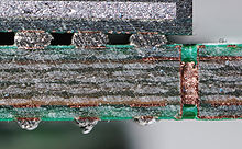
In order to do justice to the packing density in modern SMD components, especially in computers , it is not sufficient if the conductor tracks are only on one side of the circuit board. After the double-sided circuit boards, which have a copper layer on both sides of the circuit board, one began to glue several thinner circuit boards with so-called prepregs . These multi-layer so-called multilayer circuit boards can currently have up to 48 layers, in individual cases even more. Common are z. B. four to eight layers in computers and up to twelve layers in cell phones. The connections between the layers are made with plated-through holes ("vias").
In many cases, the use of multilayer circuit boards is necessary even with a lower packing density, e.g. B. to ensure the low induction power supply of all components.
Components on and in circuit boards
Simple passive components can be integrated into the board. Inductors, coils, small capacitances, contacts or heat sinks can be designed directly as a copper layer structure. Resistors can be imprinted on the surface or in the hidden layers using special pastes. This means that components and their assembly can be saved.
There are circuit boards on or in which integrated circuits are placed directly (chip on board, chip in board). They are often directly to the board bonded and only protected by a drop of resin ( English Glob Top ) (for example, quartz movements).
Microvia technology
HDI circuit board technology has now become standard for multilayer boards . In this process, blind holes with a diameter of 50 µm to 100 µm are made in the outer layers by laser or plasma etching and end on the copper of the next - or the next - layer. After the remaining resin has been cleaned, these micro-drilled holes are again galvanically copper-plated and thus connected electrically.
There are several possibilities of the layer structure,
- one layer each symmetrical,
- one layer asymmetrical,
- two layers symmetrical,
- two layers asymmetrical,
- Microvias over two layers (stacked via).
For circuit boards with a high packing density (HDI-PCB, High Density Interconnect), the microvia technology is necessary because, due to the lack of space and the small spacing of the contacts, not all contacts, e.g. B. Ball Grid Array components (BGA) could be electrically connected. In this way, the pads of the BGAs are attached to microvia bores that end on a different layer, thus ensuring that they are unbundled .
Buried via technique
The vias (plated-through holes) also connect two or more copper layers here, but are only inserted between inner layers and are not accessible from the surface of the board. Buried vias (dt .: buried vias ) are therefore only possible with multilayer boards with four or more layers.
Plugged Via technology
In addition to buried and micro vias, there is also the option of having vias closed (“plugged”). With this technique, vias can be placed directly in SMD pads. B. in BGA housings with small ball gaps, the unbundling is greatly simplified. However, the technology is relatively expensive and is rarely used, as the surface also has to be sanded and polished to remove excess material. The various options for closing a via are specified in guideline IPC 4761.
Thick copper
The use of copper thicknesses from 200 µm to 400 µm is called thick copper. They allow higher currents and lateral heat transport. Due to the etching process, only rough conductor structures can be realized.
Alternatively, a circuit board with a thin copper thickness can be structured photolithographically and galvanically reinforced with copper. Subsequent etching can then expose the conductor tracks without a masking varnish, so that not the entire copper thickness, but only the thin base layer has to be etched.
A further development of thick copper technology is the Iceberg Technology ( English iceberg technique ). The still closed copper layers are pre-structured in foil form by a photolithographic etching process: Areas that do not require thick copper are etched back to 20 µm or 100 µm. The foils are then pressed into the prepreg and conventionally processed. The remaining small elevation allows a finer structure and possibly more reliable coverage with solder mask .
Thermal management
Thermal vias improve the heat transport perpendicular to the circuit board. The thermal conductivity of inexpensive base materials such as FR-4 with 0.3 W / (m · K) is too low for heat dissipation from components. Thermal vias are plated-through holes whose primary task is to improve the thermal conductivity; they use the high thermal conductivity (300 W / (m · K)) of copper, the material of the through-hole plating. A dense arrangement, for example in a hexagonal grid of 0.5 mm and a diameter of the vias of 0.25 mm, effectively allows up to 10% copper to be introduced into the circuit board. This results in a thermal conductivity of 30 W / (m · K) perpendicular to the circuit board.
Metal core ( English metal core ) and thick copper allow a higher lateral thermal conductivity. For this purpose, copper or aluminum sheets or copper layers reinforced up to 400 µm are incorporated into the circuit board.
In connection with a thermal paste printing, a heat reduction can be achieved and in certain cases the use of additional heat sinks can be avoided; a printed circuit board in euro card format has a thermal resistance of 6 K / W due to convection and about 5 K / W due to thermal radiation .
There are also water-cooled printed circuit boards in which fine grooves are milled on the top and bottom of the inner layers before the individual layers are assembled. After assembly, there remains a channel through which cooling water can be passed.
Recently, circuit boards have also been provided with a thin copper layer on the narrow sides, which can serve to improve heat dissipation. It can also help reduce the emission of electromagnetic fields.
A secondary aspect in heat management concerns the heat distribution during soldering: EDA programs specifically set so-called thermal pads , in which the connection to copper-filled surfaces is specifically weakened in order to keep the heat in the soldering point and not distribute it to the copper surface.
Flexible circuit boards
As an alternative to fixed circuit boards, there are also thin flexible circuit boards such. B. use based on polyimide films. The flexible circuits built in this way are more expensive, but can save space by folding in the tightest structures z. B. be used in cameras , video cameras or smartphones .
Flexible connections for continuous use, e.g. B. in inkjet printers, are also often designed as a polyimide film circuit board.
- Rigid-flexible printed circuit boards
- A rigid-flexible printed circuit board is obtained by combining flexible and rigid layers during pressing. Here are z. B. Polyimide films on or between ordinary FR4 layers, which, after deep milling, result in areas of different thickness and flexibility. In this way, plugs, cables and other connecting elements can be saved, but this also makes it necessary to replace the entire rigid-flex system in the event of defects.
- Semi-flexible printed circuit boards
- If only a not permanently flexible area is required in the circuit board, e.g. B. to enable assembly in tight spaces, there is the approach of tapering the stack of layers of a printed circuit board made up of several prepregs (see below) except for a few layers by milling or pre-punched prepregs with recessed areas. The tapered area is typically provided with a permanently flexible layer of varnish and can then be bent a few times.
Press-fit technology and other soldering alternatives
Press- fit technology is an alternative to soldering the component connections on a circuit board . Elastic or rigid pins are pressed into metalized holes in the circuit board with tight tolerances. The plastic deformation of the metals involved results in safe electrical connections even without soldering. The pressing in of multi-pole plugs and threaded bolts has established itself as a main application. Another possibility arises through the use of glue . You can choose between electrically non-conductive or conductive isotropic and anisotropic adhesives. Another technique is bonding ( chip-on-board technology ). Thinned (flatter etched or ground) chips are glued or soldered to the circuit board without a housing ( chip bonding ) and connected to the corresponding contacts on the circuit board using thin wires (see wire bonding ). The chips and bonding wires bonded to printed circuit boards are protected by light-absorbing synthetic resin. An alternative to the press-fit technique, which is not soldered, is the direct plug-in technology with reversible contacts.
Surface treatment and equipment
Since there are usually transport and storage times between the circuit board production and the subsequent assembly process of the electronic components on circuit boards, it is necessary to protect the soldering surfaces made of bare copper, which represent the contacts to the electronic components, from environmental influences such as corrosion, otherwise the Soldering process is impaired. The following processes are used for surface treatment on printed circuit boards:
HAL
HAL also HASL for English Hot Air Solder Leveling , the finished printed circuit board produced is immersed in a bath of liquid tin-lead and blown hereinafter with hot air, the excess tin-lead on the surface to provide a smooth surface as possible to the solder pads to receive. This means that the copper is coated with a layer of tin-lead, which also corresponds to conventional solder. HAL is the most widespread surface treatment because it is inexpensive to carry out, but has a disadvantage due to the uneven distribution of the tin-lead coating on the surface, and it can lead to short circuits in very fine structures.
Chemical tin
In the method of chemical tin ( English Immersion Tin ), the uppermost layer of copper is by means of thiourea by tin chemically replaced. The chemical exchange of copper atoms by tin atoms ends automatically when the copper surfaces on the conductor plate are completely covered by tin to a thickness of approx. 0.7 µm to 1.2 µm. The advantage of chemical tin is the very even surface and the avoidance of problematic substances such as lead in the end product. The disadvantages are the effort and costs involved in manufacturing, the use of carcinogenic thiourea and the problem that the pure tin surface can develop whiskers .
OSP
OSP, English Organic Solderability Preservative , is a surface treatment based on organic substances such as benzotriazole , imidazole or benzimidazole which form an organometallic bond several 100 nm thick with the top copper layer and thus protect the copper from oxidation. The OSP is only thermally dissolved during the soldering process. In addition to the flat surface, the advantageous production is advantageous, but the limited storage time is disadvantageous. OSP should not be used on circuit boards with push-through components, as surface passivation in the soldering eyes is not guaranteed.
ENIG
In ENIG, English Electroless Nickel Immersion Gold , first, an approximately 3 microns to 6 microns layer electroless nickel on the copper surface applied. The nickel layer represents a barrier for gold to the copper layer, as otherwise the gold would diffuse into the copper . A 50 nm to 100 nm thick layer of chemical gold is applied to the nickel layer, while the top nickel layer is chemically exchanged for gold. The advantage of this method, in addition to the flat surface, is the comparatively long shelf life. The comparatively high process effort and the associated costs are disadvantageous. Furthermore, the gold coating of the ENIG circuit boards leads to contamination of the solder bath during wave soldering .
Standards and regulations
There are various regulations and standards for the structure and properties of circuit boards. In addition to DIN , IEC and Institute for Printed Circuits (IPC) standards, some large companies also have their own factory standards. In addition to these universal standards, there are standardized dimensions for printed circuit boards for rack systems:
- Euro card (3 U ): 160 mm × 100 mm (DIN 41494 part 2), contacted on the narrow side
- Double euro card format (6 U): 233 mm × 160 mm, contacted on the broad side.
Testing
Circuit boards are often subjected to an inspection before they are shipped and assembled. The visual control between the individual production steps (e.g. before applying a further layer) and at the end of production is usually included in the price of circuit board manufacturers.
An electrical test at the end of production is usually chargeable and requires the complete CAD data as well as a test machine that contacts and tests all signal paths. When it comes to testing machines, a distinction is made between the in-circuit tester and the flying prober . The flying probers have several individual test fingers that test the circuit boards. This technology has the great advantage that no adapters are required for contacting, so even small series can be tested cheaply. A disadvantage is the long test time for testing and that usually no 100% test is carried out with this system (too long test time). With the in-circuit tester , the printed circuit boards are tested with adapters fitted with spring pins or very fine so-called rigid needle adapters . This technique has the advantage that all test points can be contacted at once and thus a very fast test with a 100% test depth can be achieved. Today's MCA microadapters (see rigid needle adapters ) enable the contacting of the finest microelectronic structures with staggering . A disadvantage to be mentioned here is the high adapter costs, which, however, are no longer significant for larger quantities.
Completely assembled circuit boards can also be tested with an ICT test system , for which additional contact pads are often laid out, which are no longer required in later use. So that no such additional test points have to be generated, a rigid needle adapter can also be used here, which enables contact to be made with component connections, plugs or even chips.
Often only a functional check is carried out at the end of production, since the manufacturing technology of the circuit boards themselves is much more reliable than subsequent process steps.
Continuity test
The continuity test tests the circuit board for faulty and missing connections. These interruptions can be caused by mechanical damage or film defects during exposure.
- functionality
- In the continuity test, all points belonging to a network are tested against each other. No connection can be checked for single points.
The measurements can show a high-resistance result due to dirt on the contact points. Possible contamination is: dust, milling residues or oxidation on the contact surface. By contacting again (retest), these phantom errors (errors that do not exist) can often be ruled out.
With two-pole measurement, the measurement results are product-specific, e.g. B. classified as follows:
(Measuring thresholds are to be defined on a part-specific basis)
- Measurement <10 Ω → good connection
- Measurement> 10 Ω → high-resistance connection
- Measurement> 2 MΩ → interruption
For measurements of connections or resistances below 10 Ω, a four-wire measurement must often be used, so that the cable and contact resistances do not falsify the measurement result.
Short circuit test
A short circuit is a connection between two points which, according to the circuit, must not exist. Short circuits are connections that z. B. caused by tin threads, poor etching or mechanical damage to the insulation layer between the layers.
- functionality
- A test point is defined as the primary test point for each network. Then the insulation is measured between all networks.
If a circuit board has 3 networks, network 1 is measured against network 2, network 1 against network 3 and network 2 against network 3. If there are other networks, the number of measurements is as follows:
- 2 networks = 1 measurement
- 3 networks = 3 measurements
- 4 networks = 6 measurements
- 5 networks = 10 measurements
- 6 networks = 15 measurements
- N networks = N * (N-1) / 2 measurements
If an interruption is found in the continuity test, another primary point is set there and another sub-network is generated (network 3a). In this way, the circuit board can be tested 100% for short circuits.
The measurement results are interpreted product-specifically, for example as follows:
- Measurement> 2 MΩ → No short circuit
- Measurement <2 MΩ → high-resistance short circuit
- Measurement <100 Ω → short circuit
X-ray test
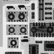
X-rays are also used, especially with multi-layer blanks, in order to be able to carry out a visual check, for example the accuracy of fit of the various layers.
Load of conductor track structures with large currents
Often, especially in thick-film hybrid technology , there is a need to test bare circuit boards with a larger test current for constrictions, poor vias, etc. Such defects are then destroyed and can be recognized as an interruption. Thermography is a non-destructive means of testing printed circuit boards, including in operation .
Base material

Simple circuit boards consist of an electrically insulating carrier material (base material) on which one or two copper layers are applied. The layer thickness is typically 35 µm and for applications with higher currents between 70 µm and 140 µm. In order to enable thinner conductor tracks, circuit boards with only 18 µm copper are also produced. In English-speaking countries, the mass of the conductive layer per unit area is sometimes given in ounces per square foot (oz / sq.ft) instead of the layer thickness. In this case 1 oz / sq.ft corresponds to about 35 µm of layer thickness.
In the past, circuit boards were mostly hard paper with the material identifier FR2. Today, apart from cheap mass-produced items, glass fiber mats impregnated with epoxy resin with the material code FR4 are mostly used. FR4 has better tracking resistance and better high frequency properties as well as lower water absorption than hard paper.
Due to the glass fiber mats, FR4 has an anisotropic structure, which is expressed, among other things, in the coefficient of linear expansion, which is 50–60 ppm / K (up to 100 ° C) perpendicular to the circuit board, and approx. 18 and 14 ppm in the X and Y directions / K, so similar to the applied copper tracks (17 ppm / K).
Other materials are also used as the base material for special applications. Examples are Teflon , aluminum oxide or ceramic in LTCC and HTCC for high-frequency technology and polyester film for flexible printed circuit boards. Manufacturers of these special base materials are companies such as Rogers Corporation and Arlon Materials for Electronics , from which the colloquial term “ Rogers ” or “ Arlon ” in technical English for Teflon-based printed circuit boards with applications in high-frequency technology is derived.
For circuit boards with high demands on heat dissipation, base materials with metal cores such as aluminum or copper are used, e.g. B. in the field of lighting technology with high-performance light emitting diodes . These carrier materials are also referred to as direct bonded copper or as insulated metal substrate (IMS).
In the case of applications for low temperatures or high humidity, base materials with integrated heating elements can also be used to prevent overcooling or condensation on the circuit. In addition, research is being carried out into alternative materials that are more environmentally friendly, but there are currently still problems with moisture resistance.
Parameters of various materials
| designation | Reinforcement | matrix | Costs rel. to FR4 |
Softening point T G 1 (° C) |
Max. Operating temperature 2 (° C) |
Dielectric constant ε r |
Insulation resistance |
Leakage current behavior |
Loss angle (degree) |
|---|---|---|---|---|---|---|---|---|---|
| FR2 | paper | Phenolic resin | 30% | 80 | 70 | 4.25 | - - | - - | 0.05 at? MHz |
| FR3 | paper | Epoxy resin (epoxy) | 60% | 100 | 90 | + - | + - | 0.041 at? MHz | |
| CEM1 | paper | Epoxy | 70% | 105 | + - | + - | 0.031 at? MHz | ||
| CEM3 | Glass fleece | Epoxy | 80% | 120 | + | + | |||
| FR4 standard | Fiberglass fabric | Di / tetra epoxy | 100% | 125-150 | 115-140 | 3.8-4.5 | + | + | 0.019 at? MHz |
| FR4 halogen free | Fiberglass fabric | Di / tetra epoxy | 130% | 125-180 | 115-170 | 3.8-4.5 | + | + | 0.019 at? MHz |
| FR5 | Fiberglass fabric | Tetra / Multi-Epoxy | 150% | 150-185 | 140-175 | 0.016 at? MHz | |||
| FR5 BT | Fiberglass fabric | BT epoxy | 300% | 190-240 | |||||
| Polyimide | with or without glass fibers | Polyimide | 332-438% | 240-270 | 230-260 | + | + | ||
| Teflon (PTFE) | without or glass fibers | 800% | 260-320 | 250-310 | 2-2.28 | + + | + + | 0.0009 (10 GHz) ... 0.03 (10 GHz) |
|
| Ceramic ( aluminum oxide ) |
- | 800% | Not relevant | Not relevant | 7 (4.5-8.4 8) |
+ + | + + |
Base material production
First the base resin, solvent, hardener and accelerator are mixed in the impregnation system. Other substances can also be added to this, such as B. Color pigments, flame retardants and flexibilizers. The carrier materials (e.g. paper, glass fabric, aramid fabric ) are delivered in rolls so that the process can be carried out continuously. After the carrier has been pulled through the bath over pulleys (impregnation), the material is dried in the oven. Not only does the solvent evaporate, but the resin also reaches an intermediate state due to the supply of heat - the resin does not yet harden completely, when the heat is applied again it initially becomes sticky again and only then hardens. This semi-finished product made of resin and carrier is called prepreg. It is used to manufacture the circuit boards by pressing the layers under the influence of heat. With multilayer circuit boards, several layers of base material and copper are pressed and etched one after the other.
links
Mechanical connections
When assembling circuit boards in a housing, a distance must be ensured between the possibly metal mounting base and the circuit board. On the one hand, so that there are no short circuits , and on the other hand, so that the uneven underside of the board with the many soldering points and sometimes protruding wire ends does not lie directly, which would lead to mechanical stresses. For this one uses u. a. long threaded screws with spacers and nuts or plastic elements that are clipped into holes in the board and on the other side in the housing. Sometimes the electrical connection described below also takes on the mechanical part.
Electrical connections
If the circuit board is a plug-in card that sits on another circuit board, direct connectors and socket strips are usually used .
Other multi-pole cable connections are made using conductive rubber or plug strips and pin strips, whereby the contacts can be arranged in one or more rows. If only a few poles are involved, socket strips or small socket or coupling parts are also plugged onto solder pins .
In special environments, such as within mechanical cameras , foil connectors are chosen that represent practically flexible printed circuit boards, possibly with direct plug connectors at one or both ends or alternatively direct soldering.
recycling
Printed circuit boards contain a high proportion of copper, which has become economical to recover thanks to advances in recycling processes:
| element | Mobile phones | computer | Mixed fraction |
|---|---|---|---|
| copper | 34.49 | 20.19 | 20.1 |
| aluminum | 0.26 | 5.7 | 13.5 |
| iron | 10.57 | 7.33 | 7.09 |
| zinc | 5.92 | 4.48 | 2.18 |
| lead | 1.87 | 5.53 | 1.16 |
| tin | 3.39 | 8.83 | 0.62 |
| nickel | 2.63 | 0.43 | 0.73 |
| silver | 0.21 | 0.16 | 0.027 |
| gold | 0 | 0.13 | 0.003 |
literature
- Günther Hermann (Hrsg.): Manual of printed circuit board technology - Laminate - Manufacturing - Assembly - Test . 2nd Edition. Eugen G. Leuze Verlag, Saulgau / Württ. 1982, ISBN 3-87480-005-9 .
- Günther Hermann (Hrsg.): Handbuch der Leiterplattenentechnik - Volume 2: New processes, new technologies . Eugen G. Leuze Verlag, Saulgau / Württ. 1991, ISBN 3-87480-056-3 .
- Günther Hermann (Hrsg.): Handbuch der Leiterplattenentechnik - Volume 3: Circuit board technology, manufacture and processing, product liability, environmental protection technology with disposal . Eugen G. Leuze Verlag, Saulgau / Württ. 1993, ISBN 3-87480-091-1 .
- Günther Hermann (Ed.): Handbuch der Leiterplattenentechnik - Volume 4: With 112 tables . Eugen G. Leuze Verlag, Saulgau / Württ. 2003, ISBN 3-87480-184-5
- H.-J. Hanke (Hrsg.): Assembly technology of electronics - printed circuit boards . Technik Verlag, Berlin 1994, ISBN 3-341-01097-1 .
- Daniel Schöni (Ed.): Circuit and PCB design in detail - from the idea to the finished device . BoD Books on Demand, Norderstedt 2017, ISBN 978-3-7392-1871-7 .
See also
Web links
- Inexpensive production of circuit boards with simple means
- Etch circuit boards with the "direct toner method"
Individual evidence
- ↑ Material flows in the manufacture of printed circuit boards. ( Memento of the original from January 15, 2015 in the Internet Archive ) Info: The archive link was automatically inserted and not yet checked. Please check the original and archive link according to the instructions and then remove this notice. (PDF; 729 kB) Research Center Karlsruhe 1996.
- ↑ Paul Eisler, Harold Vezey Strong: "639.178 (A) Manufacture of electric circuits and circuit components".
- ↑ Andus Electronic PCBs Current rating on PCBs Basics and practical knowledge.
- ↑ Eilhard Haseloff: EMC-compliant and just design of printed circuit boards , Texas Instruments Germany, application laboratory, publication EB215, May 1993
- ↑ EEVblog # 1176 - 2 Layer vs 4 Layer PCB EMC TESTED!
-
↑ 1115 hits for emv jobs on StepStone ; selected pages of search hits:
- first page ( Memento from January 4, 2020 in the web archive archive.today ),
- second page ( memento of January 4, 2020 in the web archive archive.today ),
- third page ( memento of January 4, 2020 in the web archive archive.today ),
- fourth page ( Memento from January 4, 2020 in the web archive archive.today ),
- fifth page ( memento of January 4, 2020 in the web archive archive.today ).
- ↑ microcirtec.de .
- ↑ Design rules plugging (PDF; 272 kB) ( page no longer available , search in web archives ) Info: The link was automatically marked as defective. Please check the link according to the instructions and then remove this notice. (PDF) ILFA Feinstleitertechnik; with process description and illustrations.
- ↑ Via cover - specification according to IPC 4761 . Multi CB circuit boards; with illustrations.
- ↑ Circuit and PCB design in detail. Retrieved April 22, 2017 .
- ↑ we-online.de Retrieved on December 2, 2014.
- ^ Al Wright: Printed Circuit Board Surface Finishes - Advantages and Disadvantages. Retrieved July 9, 2016 .
- ↑ Analysis with DDK, TMA and TGA-EGA. In: USER COM 1/99. Retrieved January 18, 2020 .
- ↑ Alternative board materials. ( Memento from May 15, 2008 in the Internet Archive )
- ↑ High Tg (Glass Transition Temperature). Unicircuit.
- ↑ a b mauritz-hamburg.de ( Memento from October 22, 2014 in the Internet Archive ) Duorid 5880, glass fiber reinforced.
- ^ Basics of radar technology for level measurement ( Memento from October 26, 2007 in the Internet Archive ), 9
- ↑ quick-ohm.de ( Memento from May 24, 2010 in the Internet Archive ).
- ↑ Luciana Harue Yamane, Viviane Tavares de Moraes, Denise Crocce Romano Espinosa, Jorge Alberto Soares Tenório: Recycling of WEEE: Characterization of spent printed circuit boards from mobile phones and computers . In: Waste Management . tape 31 , no. December 12 , 2011, p. 2553-2558 , doi : 10.1016 / j.wasman.2011.07.006 .
