Intel 80386
| << Intel 80386 >> | |
|---|---|
 Intel i386DX, 16 MHz |
|
| Production: | 1985 to 2007 |
| Producers: | |
| Processor clock: | 12 MHz to 40 MHz |
| L1 cache size: | 0 KiB |
| Manufacturing : | 1.5 µm to 1.0 µm, CMOS |
| Instruction set : | x86 (16 bit) and x86-32 |
Base:
|
|
The 80386 is an x86 CPU that was developed by Intel under the brand name i386 (initially iAPX 386 ) as the successor to the 80286 and was produced from 1985 to September 2007. The 386 - as the 80386 is often called (pronounced eighty-six ) - was later copied by AMD and sold as the Am386 , while Chips & Technologies developed its own compatible version. IBM licensed the i386SX and developed the improved IBM 386SLC from it .
Historical meaning
With the 80386, Intel made the change to the 32-bit architecture ( IA-32 , often also called i386), the functions of which are still available in all successor models up to the Core i9 (as of 2019) and which are also used by other manufacturers as a template for own processors served. The registers of this processor family and the address space of the architecture are 32 bits wide. The 80386 is still used today for control tasks (e.g. telephone exchange systems) and in the aerospace industry.
From 1982, development at Intel was headed by John Crawford .
architecture
variants
There were a total of four versions of this CPU, which differed in terms of data bus and purpose. Production of the i386EX as an embedded version of the i386SX was only discontinued in 2007.
- Intel386SX
A variant of the 80386 is the 80386SX . It only has a 16-bit external data bus and a 24-bit address bus , but internally retains the 32-bit micro- architecture of the 80386. The 24-bit address bus limits the addressable physical memory of the 386SX to 16 MiB ; In view of the usual memory expansion in the home sector of mostly a maximum of 4 MiB at the beginning of the 1990s, this was not a serious limitation, especially since many 386SX mainboards also did not allow a memory expansion of 16 MiB. From the programmer's point of view, apart from the memory limitation, there is practically no difference between the 386SX and the "real" 80386, which was renamed the 80386DX to distinguish it from its little brother after its introduction. Due to the reduced data bus width and the lower available clock frequencies, the 386SX only achieves a significantly lower execution speed than the 386DX.
- Intel386SL
The Intel386SL is a version of the i386SX designed for portable computers. With it, the System Management Mode (SMM) was introduced, which can put the CPU into deep sleep to save energy.
- RapidCad
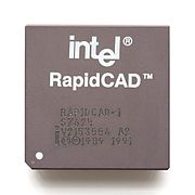
The RapidCad was an upgrade for 386 systems based on 486 technology. The RapidCad consisted of two chips, the RapidCad1 and the RapidCad2, the former replacing the 80386 CPU and the latter replacing the 80387 coprocessor . The RapidCad2 did not contain the electronics of the coprocessor, but only a logic for generating external bus signals. The actual coprocessor was already integrated in the RapidCad1.
Compared to an i386 system with an i387 coprocessor, the RapidCad brought - depending on the application - a moderate increase in performance of around 30 percent; However, the performance did not come close to a system with an 80486 processor. In addition to the high price, this fact also ensured that the RapidCad was not widely used, which is why the two chips are coveted collector's items today.
Segments
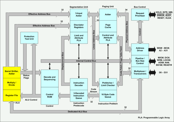
The 80386 can directly address up to 4 GiB main memory (386SX: 16 MiB). The logical address space is 2 46 bytes = 64 TiB, which can only be used in full in theory. In protected mode, the processor uses segmented memory addressing with 16 bit wide selectors and - depending on the operating mode - 16 or 32 bit wide offsets.
The segmentation unit supports four privilege levels, which are intended for the following tasks:
- Ring 0 - for the kernel and device drivers
- Ring 1 - rarely used for drivers that do not require unlimited hardware access (e.g. file system drivers)
- Ring 2 - for system services
- Ring 3 - for the execution of normal applications
Only a few PC operating systems have used these four privilege levels. Usually (also due to the compatibility with other processor architectures that only have two privilege levels) only ring 0 (for kernel and (basic) driver) and ring 3 (for all other code) are used.
In terms of security, protected mode is clearly superior to the flat addressing model that has now become established. Nevertheless, almost all of the newer PC operating systems exclusively use the “flat memory” model for application programs. This simplifies programming and can be transferred to other processor architectures that do not have a segmentation unit.
On the hardware side, segmentation and paging can also be used in parallel . First the linear address is calculated by segmentation and then converted into the physical address via paging. Without paging, the linear address corresponds to the physical address.
When using a so-called “flat memory” model, in which data, code and stack segments are displayed in a linear 4 GiB address space of the application programs, the memory within the application programs can be addressed using simple 32-bit offsets. This bypasses the memory protection offered by the segmentation unit. In the x64 mode of the newer 64-bit processors introduced by AMD , no expansion of the segmentation was provided, so that only a “flat memory” model can be used.
The paging unit allows only a relatively simple, page-based memory protection. In the meantime, attempts are being made to address the security gaps associated with the “flat memory” model with new hardware extensions such as NX-Bit (from AMD Athlon 64) or SMEP.
Paging
To manage now serves an additional level which 4 KiB large memory pages used (English memory pages). The base addresses of all pages are recorded in page tables. These are stored in page directories with 1024 entries. An address space of size 4 GiB is therefore divided into 1024 × 1024 pages of 4 KiB. The linear 32-bit address can be divided into three parts:
- 12 bit offset in the memory page
- 10 bit index on page table
- 10 bit index on the page directory
There are two privilege levels at the page level:
- Supervisor mode - for operating system and driver (ring 0, 1 and 2)
- User mode - for application programs (ring 3)
The equivalent of the segment privileges is given in brackets.
register
It has eight general 32-bit registers, some of which have special purposes in connection with various commands, but otherwise can be used freely for computing and general data exchange:
| Abbr. | Surname | Special use |
|---|---|---|
| EAX | Accumulator | least significant part and first operand for multiplication; Quotient in division; BCD commands |
| EBX | Base register | None (The 16-bit register BX could be used in 16-bit mode for index addressing; in 32-bit mode this is possible with all “General Purpose” registers.) |
| ECX | Count Register | Loop counter for JCXZ and LOOP; Shift distance of shift commands |
| EDX | Data register | higher part in case of multiplication; Remainder at division; Port address for the commands IN reg, DX and OUT DX, reg |
| EBP | Base pointer | Is used to address the stack frame for local variables / parameter transfer. |
| ESP | Stack pointer | Pointer to the current position in the stack segment; Can only be used to a limited extent, since this register specifies where the return address of subroutines and interrupts is stored. |
| IT I | Source Index | Source for string operations |
| EDI | Destination index | Target for string operations |
There are also other registers for controlling the behavior of the CPU:
| Abbr. | Surname | use |
|---|---|---|
| EIP | Instruction pointer | Points to the next command to be executed. |
| EFLAGS | Flag Register | The individual bits have different meanings and show e.g. B. overflows in arithmetic operations u. Ä. on. |
| CS | Code segment | Segment selector of the code segment (in which the currently executing program code is located) |
| DS | Data segment | Segment selector of the data segment (in which the global data of the program are located) |
| SS | Stack segment | Segment selector of the stack segment (in which the stack for the local data and return addresses are located) |
| IT | Extra segment | Segment selector of another data segment (used e.g. for string copy commands) |
| FS and GS | Extra segment 2 and 3 | Segment selectors of two further data segments |
| GDTR | Global Descriptor Table Register | Stores linear address and size of the GDT |
| LDTR | Local Descriptor Table Register | Segment selector for the segment that contains the currently active LDT (there can be several LDT entries in the GDT at the same time) |
| IDTR | Interrupt Descriptor Table Register | Stores the linear address and size of the IDT |
| CR0 ... CR3 | Control Register 0 ... 3 | Taxes and A. the paging , the coprocessor and the protected mode (the lower 16 bits of the CR0 are the MSW adopted by the 80286) |
| TR6 ... TR7 | Test register 6 ... 7 | To check the translation lookaside buffer (TLB). |
| DR0 ... DR7 | Debug register 0 ... 7 | Used to set four breakpoints at processor level (DR0 ... DR3) and similar. a. |
| TR | Task register | Segment selector of the active task status segment (TSS) (several TRs can be in the GDT and LDT at the same time) |
All general purpose registers, as well as EIP and EFLAGS, are extended to 32 bits (the E comes from the English extended ) versions of the corresponding 16-bit registers of the predecessors 8086 to 80286 .
Processor bugs
POPA / POPAD bug
This error occurs with all 386s. If an instruction follows immediately after the POPA or POPAD instruction in which a memory address is calculated from a base and index register, the value in the EAX register is undefined. If EAX is used as a base or index register for memory access, the processor hangs (only POPA). The Linux kernel runs a test when it boots and issues the message Checking for popad bug ... Buggy if there is an error . off, but then continues to boot.
Review of the limit of the TSS
The processor checks whether the size of the Task Status Segment (TSS) entered is large enough. Exception 10 is always triggered if the TSS is smaller than 101 bytes, but should actually trigger if the TSS is smaller than 103 bytes.
Model data
i386DX
- L1 cache: does not exist
- L2 cache: depends on the mainboard
- Design: PGA or PQFP with 132 pins
- Operating voltage ( VCore ): 5 V
- Release DATE: October 17, 1985
- Production technology: First types CHMOS III with 1.5 µm, later CHMOS IV with 1.0 µm
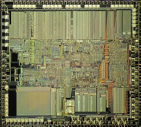
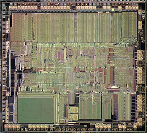
- Die-size : 104 mm² (approx. 10 mm × 10 mm, CHMOS III) and 39 mm² (6 mm × 6.5 mm, CHMOS IV)
- Number of transistors: 275,000
- Clock rates:
- 12 MHz (first models of the i386)
- 16 MHz
- 20 MHz
- 25 MHz
- 33 MHz
i386SX
- L1 cache: does not exist
- L2 cache: nonexistent
- Design: PQFP with 100 pins, PGA with 88 pins
- Operating voltage ( VCore ): 5 V
- Release DATE: June 16, 1988
- Manufacturing technology: CHMOS IV, 1.0 µm
- Die size : 104 mm² with 275,000 transistors
- Clock rates:
- 16 MHz
- 20 MHz
- 25 MHz
- 33 MHz
i386SL
Version of the i386SX for portable computers. With it, the System Management Mode (SMM) was introduced, which can put the CPU into deep sleep to save energy.
- L1 cache: does not exist
- L2 cache: 16 to 64 KiB possible
- Design: PGA with? Pins, PQFP with 132 pins
- Operating voltage ( VCore ): 5 V
- Release DATE: October 15, 1990
- Manufacturing technology: 1.0 µm
- The size :? mm² with 855,000 transistors
- Clock rates:
- 20 MHz
- 25 MHz
RapidCAD-1
- Number of transistors: 800,000
- Manufacturing process: 0.8 µm
- Cache: on-board, no on-die cache
- Architecture: 80486 technology with 80386 instruction set and pinout
- Coprocessor: Integrated
- Package: 132 pin, PGA
- Power consumption: 3.5 watts
- Clock rates: 25 and 33 MHz
RapidCAD-2
The RapidCAD-2 is a PLA for generating the FERR signal.
- Introduced: 1992
- Number of transistors: 275,000
- Manufacturing process: 0.8 µm
- Housing: 68 pin, PGA (for 387 socket)
- Clock rates: 25 and 33 MHz
i376
The i376 is an embedded processor based on the i386SX and can be regarded as the predecessor of the i386EX. It does not support real mode or paging.
- Data bus: 16 bit
- Address bus: 24 bit
- L1 cache: does not exist
- L2 cache: nonexistent
- Design: PQFP with 100 pins and PGA -88
- Operating voltage ( VCore ): 5 V
- Release DATE: January 16, 1989
- End of production: June 15, 2001
- Manufacturing technology: CHMOS IV, 1.0 µm
- The size :?
- Supported FPU: 80387SX
- Special features: boots in protected mode (does not support real mode)
- Clock rates:
- 16 MHz
- 20 MHz
i386EX, i386EXTB and i386EXTC
Embedded version of the i386SX with system and power management.
-
- Functions
- Data bus: 16 bit
- Address bus: 26 bits
- L1 cache: does not exist
- L2 cache: nonexistent
- external FPU: i387SX or i387SL
- Design : PQFP with 132 pins, SQFP with 144 pins and PGA with 168 pins
- Operating voltage ( VCore ): 2.7 V to 5.5 V.
- Release DATE: 1994
- Manufacturing technology: 0.8 µm
- The size :? mm² at? Transistors
- Clock rates:
- 16 MHz - i386EX, at 2.7 V to 3.3 V.
- 20 MHz - i386EX, at 3.0 V to 3.6 V.
- 25 MHz - i386EX, at 4.5 V to 5.5 V.
- 20 MHz - i386EXTB, at 2.7 V to 3.6 V.
- 25 MHz - i386EXTB, at 3.0 V to 3.6 V.
- 25 MHz - i386EXTC, at 4.5 V to 5.5 V.
- 33 MHz - i386EXTC, at 4.5 V to 5.5 V.
i386CXSA and i386SXSA (also as i386SXTA)
Embedded CPU with transparent power management mode, integrated MMU and TTL-compatible inputs (only SXSA version).
- Data bus: 16 bit
- Address bus: 26 bit (24 bit for i386SXSA)
- L1 cache: does not exist
- L2 cache: nonexistent
- external FPU: i387SX or i387SL
- Design: PQFP with 100 pins
- Operating voltage ( VCore ):
- 4.5 V to 5.5 V (25 and 33 MHz)
- 4.75 V to 5.25 V (40 MHz)
- Publication date:
- Manufacturing technology: CHMOS V, 0.8 µm
- The size :? mm² at? Transistors
- Clock rates:
- 25 MHz
- 33 MHz
- 40 MHz
i386CXSB
Embedded CPU with transparent power management mode and integrated MMU .
- Data bus: 16 bit
- Address bus: 26 bits
- L1 cache: does not exist
- L2 cache: nonexistent
- external FPU: i387SX or i387SL
- Design: PQFP with 100 pins
- Operating voltage ( VCore ):
- 3.0 V at 16 MHz
- 3.3 V at 25 MHz
- Publication date:
- Manufacturing technology: CHMOS V, 0.8 µm
- The size :? mm² at? Transistors
- Clock rates:
- 16 MHz
- 25 MHz
other producers


- AMD
- Chips & Technologies
- IBM


